- 您現(xiàn)在的位置:買賣IC網(wǎng) > PDF目錄385768 > RF2423 (RF MICRO DEVICES INC) 100mW SPREAD-SPECTRUM TRANSMITTER IC PDF資料下載
參數(shù)資料
| 型號: | RF2423 |
| 廠商: | RF MICRO DEVICES INC |
| 元件分類: | 無繩電話/電話 |
| 英文描述: | 100mW SPREAD-SPECTRUM TRANSMITTER IC |
| 中文描述: | TELECOM, CELLULAR, RF AND BASEBAND CIRCUIT, PDSO16 |
| 封裝: | SOP-16 |
| 文件頁數(shù): | 3/8頁 |
| 文件大?。?/td> | 67K |
| 代理商: | RF2423 |
5-37
RF2423
Rev A3 001218
5
M
U
NOT FOR NEWDESIGNS
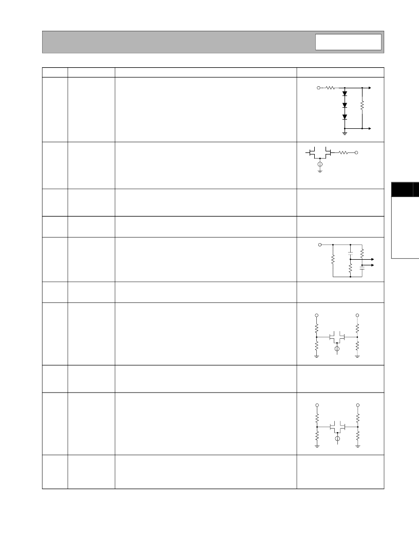
Pin
1
Function
GC
Description
Gain control of the RF amplifier. This pin can be used to control the out-
put power over a 25dB range. Output power is the lowest when the
control voltage is 1V or lower, and the highest when set to 4V or higher.
When a fixed maximum output level is needed, it is recommended to
connect this pin to VDD.
Interface Schematic
2
PHASE
This pin adjusts the phase of the I/Q signals. However, the control is
very sensitive and hard to control. Control voltage change for a few
degrees adjustment is in the order of 10mV. Device to device and tem-
perature variation are not characterized. Therefore it is not recom-
mended to use this pin; leave it not connected. Do NOT connect it to
ground. For compensating large errors in the I/Q signals supplied to the
device or in control loops, this pin may prove useful.
Power supply to all circuits except the RF output stages. It is recom-
mended to put some RF decoupling on this pin, though it is not critical.
An optional 0.1
μ
F capacitor is required if no other low frequency
bypass capacitor is nearby.
Ground connection for the gain controlled RF amplifier. Keep traces
physically short and connect immediately to ground plane for best per-
formance.
Modulator LO input. A series 22nH inductor can be used for matching.
This pin is NOT internally DC blocked. An external blocking capacitor
must be provided if the pin is connected to a device with DC present. A
DC path to ground (i.e. an inductor or resistor to ground) is, however,
acceptable at this pin. If a blocking capacitor is required, a value of
33pF is recommended.
3
VDD1
4
GND2
5
LO IN
6
GND1
Ground connection for the baseband, LO and mixer circuits. Keep
traces physically short and connect immediately to ground plane for
best performance.
Reference voltage for the I mixer. This voltage should be the same as
the DC voltage supplied to the I SIG pin. To obtain a carrier suppres-
sion of better than 25dB it may be tuned ±0.15V (relative to the I SIG
DC voltage). Without tuning, it will typically be better than 25dB. Input
impedance of this pin is about 3k
.
7
I REF
8
I SIG
Baseband input to the I mixer. This pin is DC coupled. Maximum output
power is obtained when the input signal has a peak to peak amplitude
of 5V. The DC level supplied to this pin should be VDD2/2. Input imped-
ance of this pin is about 3k
.
Baseband input to the Q mixer. This pin is DC coupled. Maximum out-
put power is obtained when the input signal has a peak to peak ampli-
tude of 5V. The DC level supplied to this pin should be VDD2/2. Input
impedance of this pin is about 3k
.
9
Q SIG
10
Q REF
Reference voltage for the Q mixer. This voltage should be the same as
the DC voltage supplied to the Q SIG pin. To obtain a carrier suppres-
sion of better than 25dB it may be tuned ±0.15V (relative to the Q SIG
DC voltage). Without tuning it will typically be better than 25dB. Input
impedance of this pin is about 3k
.
10 k
5 k
GC
PHASE
4 k
LO IN
1 k
2 k
2 k
I SIG
I REF
1 k
1 k
2 k
2 k
Q SIG
Q REF
1 k
相關(guān)PDF資料 |
PDF描述 |
|---|---|
| RF2424 | UHF QUADRATURE MODULATOR |
| RF2425 | 4-PORT TRANSFER SWITCH |
| RF2436 | TRANSMIT/RECEIVE SWITCH |
| RF2442 | HIGH-LINEARITY LOW NOISE AMPLIFIER |
| RF2444 | HIGH FREQUENCY LNA/MIXER |
相關(guān)代理商/技術(shù)參數(shù) |
參數(shù)描述 |
|---|---|
| RF2423-000 | 功能描述:可復(fù)位保險絲 RoHS:否 制造商:Bourns 電流額定值: 電阻:7.5 Ohms 最大直流電壓: 保持電流:0.1 A 安裝風(fēng)格:SMD/SMT 端接類型:SMD/SMT 跳閘電流:0.6 A 引線間隔: 系列:MF-PSHT 工作溫度范圍:- 40 C to + 125 C |
| RF2424 | 制造商:RFMD 制造商全稱:RF Micro Devices 功能描述:UHF QUADRATURE MODULATOR |
| RF2424-000 | 功能描述:可復(fù)位保險絲 RoHS:否 制造商:Bourns 電流額定值: 電阻:7.5 Ohms 最大直流電壓: 保持電流:0.1 A 安裝風(fēng)格:SMD/SMT 端接類型:SMD/SMT 跳閘電流:0.6 A 引線間隔: 系列:MF-PSHT 工作溫度范圍:- 40 C to + 125 C |
| RF-2424D | 制造商:RECOM 制造商全稱:Recom International Power 功能描述:ECONOLINE - DC/DC - CONVERTER |
| RF-2424DH | 制造商:RECOM 制造商全稱:Recom International Power 功能描述:ECONOLINE - DC/DC - CONVERTER |
發(fā)布緊急采購,3分鐘左右您將得到回復(fù)。