- 您現(xiàn)在的位置:買賣IC網(wǎng) > PDF目錄373262 > RF2431 RF Mixer PDF資料下載
參數(shù)資料
| 型號: | RF2431 |
| 英文描述: | RF Mixer |
| 中文描述: | RF混頻器 |
| 文件頁數(shù): | 2/10頁 |
| 文件大小: | 146K |
| 代理商: | RF2431 |
8-44
RF2431
Rev B1 010329
8
F
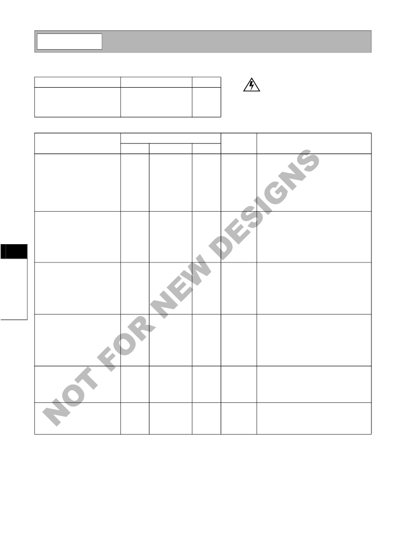
Absolute Maximum Ratings
Parameter
Supply Voltage
Input LO and RF Levels
Operating Ambient Temperature
Storage Temperature
Rating
-0.5 to 7.0
+6
-40 to +85
-40 to +150
Unit
V
DC
dBm
°C
°C
Parameter (1800MHz)
Specification
Typ.
Unit
Condition
Min.
Max.
Overall
T=25°C, V
CC
=5V, RF=1800MHz,
LO=0dBm
RF Frequency Range
IF Frequency Range
Cascade Gain
1500 to 2500
DC to 400
23
19
-14
3.5
MHz
MHz
dB
dB
dBm
dB
IF=100MHz, 50
load
IF=350MHz, 50
load
Referenced to the input
Single sideband
15
Cascade IP3
Cascade Noise Figure
First Section (LNA)
Noise Figure
Input VSWR
Input IP3
Gain
Reverse Isolation
Output VSWR
Second Section (RF Amp,
Mixer, IF1)
Noise Figure
Input VSWR
Input IP3
Conversion Gain
Output Impedance
Second Section (RF Amp,
Mixer, IF2)
Noise Figure
Input VSWR
Input IP3
Conversion Gain
Output VSWR
LO Input
LO Level
LO to RF Rejection
LO to IF Rejection
LO Input VSWR
Power Supply
Voltage
Current Consumption
2.6
2.5:1
+2
13
30
1.5:1
dB
No external matching
dBm
dB
dB
No external matching
High impedance output, 1.3k
load
9.5
1.7:1
-1
6
4
dB
Single sideband
dBm
dB
k
Open drain
Buffered output, 50
load
9.5
1.7:1
-1
6
1.2:1
dB
Single sideband
dBm
dB
-6 to +6
15
25
1.5:1
dBm
dB
dB
3 to 6.5
19
13
V
25
mA
mA
V
DD
=5.0V, LNA On, Mixer On, Buffer On
V
DD
=5.0V, LNA On, Mixer On, Buffer Off
Caution!
ESD sensitive device.
RF Micro Devices believes the furnished information is correct and accurate
at the time of this printing. However, RF Micro Devices reserves the right to
make changes to its products without notice. RF Micro Devices does not
assume responsibility for the use of the described product(s).
相關(guān)PDF資料 |
PDF描述 |
|---|---|
| RF2450 | Analog IC |
| RF2454 | RF Modulator |
| RF2464 | RF Modulator |
| RF24 | Analog IC |
| RF250 | Quadrature Demodulator |
相關(guān)代理商/技術(shù)參數(shù) |
參數(shù)描述 |
|---|---|
| RF2432-000 | 功能描述:可復(fù)位保險絲 RoHS:否 制造商:Bourns 電流額定值: 電阻:7.5 Ohms 最大直流電壓: 保持電流:0.1 A 安裝風(fēng)格:SMD/SMT 端接類型:SMD/SMT 跳閘電流:0.6 A 引線間隔: 系列:MF-PSHT 工作溫度范圍:- 40 C to + 125 C |
| RF2436 | 制造商:RFMD 制造商全稱:RF Micro Devices 功能描述:TRANSMIT/RECEIVE SWITCH |
| RF2436_06 | 制造商:RFMD 制造商全稱:RF Micro Devices 功能描述:TRANSMIT/RECEIVE SWITCH |
| RF2436_1 | 制造商:RFMD 制造商全稱:RF Micro Devices 功能描述:TRANSMIT/RECEIVE SWITCH |
| RF2436PCBA | 制造商:RFMD 制造商全稱:RF Micro Devices 功能描述:TRANSMIT/RECEIVE SWITCH |
發(fā)布緊急采購,3分鐘左右您將得到回復(fù)。