- 您現(xiàn)在的位置:買賣IC網(wǎng) > PDF目錄385769 > RF2609 (RF MICRO DEVICES INC) USB A-PIGTAIL SUB-CH.1310MM PDF資料下載
參數(shù)資料
| 型號: | RF2609 |
| 廠商: | RF MICRO DEVICES INC |
| 元件分類: | 衰減器 |
| 英文描述: | USB A-PIGTAIL SUB-CH.1310MM |
| 中文描述: | 12 MHz - 175 MHz RF/MICROWAVE WIDE BAND LOW POWER AMPLIFIER |
| 封裝: | PLASTIC, SSOP-16 |
| 文件頁數(shù): | 3/8頁 |
| 文件大?。?/td> | 94K |
| 代理商: | RF2609 |
10-11
RF2609
Rev B3 000822
10
I
NOT FOR NEWDESIGNS
SeeUpgradedProductsRF2619& RF2629
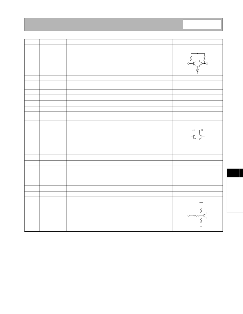
Pin
1
Function
CDMA+
Description
CDMA Balanced Input Pin. This pin is internally DC biased and should
be DC blocked if connected to a device with a DC level, other than V
CC
,
present. A DC to connection to V
CC
is acceptable. For single-ended
input operation, one pin is used as an input and the other CDMA input
is AC coupled to ground. The balanced input impedance is 1k
, while
the single-ended input impedance is 500
.
Interface Schematic
2
3
CDMA-
GND
Same as pin 2, except complementary input.
See pin 1 schematic.
Ground connection. Keep traces physically short and connect immedi-
Same as pin 3.
4
5
6
7
8
GND
GND
GND
GND
NC
Same as pin 3.
Same as pin 3.
Same as pin 3.
No Connection pin. This pin is internally biased and should not be con-
nected to any external circuitry, including ground or V
CC
.
Balanced Output pin. This is an open-collector output, designed to
operate into a 500
balanced load. The load sets the operating imped-
ance, but an external choke or matching inductor to V
CC
must also be
supplied in order to correctly bias this output. This bias inductor is typi-
cally incorporated in the matching network between the output and next
stage. Because this pin is biased to V
CC
, a DC blocking capacitor must
be used if the next stage’s input has a DC path to ground.
Same as pin 9, except complementary output.
9
OUT-
10
11
12
13
OUT+
GND
GND
VCC
See pin 9 schematic.
Same as pin 3.
Same as pin 3.
Supply Voltage pin. External bypassing is required. The trace length
between the pin and the bypass capacitors should be minimized. The
ground side of the bypass capacitors should connect immediately to
ground plane. Pins 13, 14, and 15 may share one bypass capacitor if
trace lengths are kept minimal.
Same as pin 13.
14
15
16
VCC
VCC
GC
Same as pin 13.
Analog gain adjustment for all amplifiers. Valid control ranges are from
0V to 3.0V. Maximum gain is selected with 3.0V. Minimum gain is
selected with 0V. These voltages are valid only for a 3.3k
DC source
impedance.
580
V
CC
580
CDMA-
CDMA+
OUT-
OUT+
23.5 k
15 k
12.7 k
V
CC
相關(guān)PDF資料 |
PDF描述 |
|---|---|
| RF2617 | LEAD, DVI-D TO DVI-D DUAL LINK, 2M; Connector type A:DVI-D; Connector type B:DVI-D; Length, lead:2m; Cable type:Shielded; Ways, No. of:24; Series:MICROCROSS RoHS Compliant: Yes |
| RF2619 | 3V CDMA/FM TRANSMIT AGC AMPLIFIER |
| RF2627 | 3V CDMA RECEIVE AGC AMPLIFIER |
| RF2629 | 3V CDMA/FM TRANSMIT AGC AMPLIFIER |
| RF2637 | RECEIVE AGC AMPLIFIER |
相關(guān)代理商/技術(shù)參數(shù) |
參數(shù)描述 |
|---|---|
| RF2609-000 | 制造商:TE Connectivity 功能描述:POLYSWITCH 0.10A RESET FUSE SMD |
| RF2611-000 | 制造商:TE Connectivity 功能描述:FUSE 40A 30V FAST ACTING 2PIN - Bag 制造商:TE Connectivity 功能描述:RUEF300 |
| RF2614-000 | 制造商:TE Connectivity 功能描述:RXEF050-AP - Ammo Pack |
| RF2617 | 制造商:RFMD 制造商全稱:RF Micro Devices 功能描述:3V CDMA/FM RECEIVE AGC AMPLIFIER |
| RF2618-000 | 制造商:TE Connectivity 功能描述:POLYZEN - Tape and Reel 制造商:TE Connectivity 功能描述:POLYZEN - Cut TR (SOS) 制造商:TE Connectivity 功能描述:TVS POLYZEN SMD 制造商:TE Connectivity / Raychem 功能描述:TVS POLYZEN SMD |
發(fā)布緊急采購,3分鐘左右您將得到回復(fù)。