- 您現(xiàn)在的位置:買賣IC網(wǎng) > PDF目錄385769 > RF2705 (RF MICRO DEVICES INC) 887664300 PDF資料下載
參數(shù)資料
| 型號(hào): | RF2705 |
| 廠商: | RF MICRO DEVICES INC |
| 元件分類: | 無(wú)繩電話/電話 |
| 英文描述: | 887664300 |
| 中文描述: | TELECOM, CELLULAR, RF AND BASEBAND CIRCUIT, PQCC24 |
| 封裝: | 4 X 4 MM, PLASTIC, QFN-24 |
| 文件頁(yè)數(shù): | 12/24頁(yè) |
| 文件大小: | 379K |
| 代理商: | RF2705 |
第1頁(yè)第2頁(yè)第3頁(yè)第4頁(yè)第5頁(yè)第6頁(yè)第7頁(yè)第8頁(yè)第9頁(yè)第10頁(yè)第11頁(yè)當(dāng)前第12頁(yè)第13頁(yè)第14頁(yè)第15頁(yè)第16頁(yè)第17頁(yè)第18頁(yè)第19頁(yè)第20頁(yè)第21頁(yè)第22頁(yè)第23頁(yè)第24頁(yè)
5-124
RF2705
Rev A4 041026
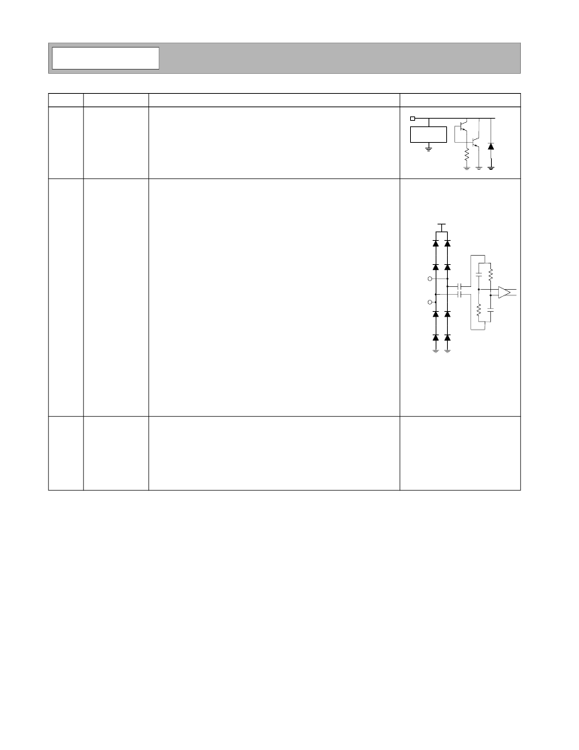
Pin
1
Function
VCC2
Description
Supply for LO buffers, frequency doubler and dividers.
Interface Schematic
2
LO HB P
High band local oscillator input (1800MHz).
In “l(fā)ow band F
LO
/2” modes the signal (LOHBP-LOHBN) undergoes a
frequency division of 2 to provide the low band LO signal for the modu-
lator.
In “high band F
LO
x1” modes the signal (LOHBP-LOHBN) is used as
the high band LO signal for the modulator.
In “high band bypass” a modulated DCS1800/PCS1900 signal
(LOHBP-LOHBN) is switched into the RF signal path. The modulator
is disabled and the signal is routed to the RFOutHb outputs through a
differential PA driver amplifier.
The LOHBP input is AC-coupled internally.
The noise performance, carrier suppression at low output powers and
sideband suppression all vary with LO power. The optimum LO power
is between -3dBm and +3dBm. The device will work with LO powers as
low as -20dBm however this is at the expense of higher phase noise in
the LO circuitry and poorer sideband suppression.
The input impedance should be externally matched to 50
. The port
can be driven either differentially or single ended. The port impedance
does not vary significantly between active and power down modes.
The RF2705 is intended for use with the RF6002. This performs the
GSM GMSK modulation within a Frac-N synthesizer loop. The 8PSK
EDGE and W-CDMA signal modulations are performed in the RF2705
and uses the RF6002’s synthesizers to generate the LO signals. The
LO signal for EDGE900 mode is derived by frequency division by 2 of
the RF6002’s DCS1800 VCO. This helps protect the system against PA
pulling.
The complementary LO input for both LOHBP LO signals.
In any of the modes the LOHB input may be driven either single ended
or differentially. If the LO is driven single ended then the PCB board
designer can ground this pin.
It is recommended that if this pin is grounded that it is kept isolated
from the GND1 pin and the die flag ground. All connections to any other
ground should be made through a ground plane. Poor routing of this
ground signal can significantly degrade the LO leakage performance.
3
LO HB N
See pin 2.
Modulator and
VGA
VCC2
LO HB P
LO HB N
V
CC
相關(guān)PDF資料 |
PDF描述 |
|---|---|
| RF2705PCBA-41X | 887664400 |
| RF2713 | 887667300 |
| RF2721 | QUADRATURE DEMODULATOR |
| RF2909 | 3V 915MHZ SPREAD-SPECTRUM TRANSMITTER IC |
| RF2915 | 433/868/915MHZ FSK/ASK/OOK TRANSCEIVER |
相關(guān)代理商/技術(shù)參數(shù) |
參數(shù)描述 |
|---|---|
| RF2705-000 | 制造商:TE Connectivity 功能描述:FUSE 40A 72V RESETTABLE - Bag |
| RF2705G | 制造商:RFMD 制造商全稱:RF Micro Devices 功能描述:LOW NOISE, MULTI-MODE, QUAD-BAND, QUADRATURE MODULATOR AND PA DRIVER |
| RF2705G_1 | 制造商:RFMD 制造商全稱:RF Micro Devices 功能描述:LOW NOISE, MULTI-MODE, QUAD-BAND, QUADRATURE MODULATOR AND PA DRIVER |
| RF2705GPCBA-41X | 制造商:RFMD 制造商全稱:RF Micro Devices 功能描述:LOW NOISE, MULTI-MODE, QUAD-BAND, QUADRATURE MODULATOR AND PA DRIVER |
| RF2705PB005 | 制造商:Hubbell Wiring Device-Kellems 功能描述:HAZ LOC LINKOSITY FEM, 5W, 20A |
發(fā)布緊急采購(gòu),3分鐘左右您將得到回復(fù)。