- 您現(xiàn)在的位置:買賣IC網(wǎng) > PDF目錄385769 > RF2909 (RF MICRO DEVICES INC) 3V 915MHZ SPREAD-SPECTRUM TRANSMITTER IC PDF資料下載
參數(shù)資料
| 型號: | RF2909 |
| 廠商: | RF MICRO DEVICES INC |
| 元件分類: | 無繩電話/電話 |
| 英文描述: | 3V 915MHZ SPREAD-SPECTRUM TRANSMITTER IC |
| 中文描述: | TELECOM, CELLULAR, RF AND BASEBAND CIRCUIT, PDSO24 |
| 封裝: | SSOP-24 |
| 文件頁數(shù): | 4/8頁 |
| 文件大?。?/td> | 156K |
| 代理商: | RF2909 |
11-106
RF2909
Rev B1 010904
11
T
SeeUpgradedProductRF2942
transmitter is turned on. Buffer amp is off when < 1V.
GND3
Ground connection for RF Power Amp. Keep traces physically short
and connect immediately to ground plane for best performance.
GND4
Same as pin16.
Pin
1
Function
Q SIG
Description
Baseband input to the Q mixer. A DC bias of approximately 1.7V is
present at this pin.A DC blocking capacitor is needed if the signal has a
different DC level. Maximum output power is obtained when the input
signal has a peak-to-peak amplitude of 1V. The input impedance of this
pin is 3k
. The REF and SIG inputs are interchangeable. If swapping
the I SIG and I REF pins, the Q SIG and Q REF also need to be
swapped to maintain the correct phase. The SIG and REF pins may be
driven deferentially to increase conversion gain.
Reference voltage for the Q mixer. This voltage should be the same as
the DC voltage supplied to the Q SIG pin. To obtain a carrier suppres-
sion of better than 25dB it may be tuned ±0.15V (relative to the Q SIG
DC voltage). Without tuning, the carrier suppression will typically be
better than 25dB. The input impedance of this pin is about 3 k
.
Ground connection for the modulator circuits. Keep traces physically
short and connect immediately to ground plane for best performance.
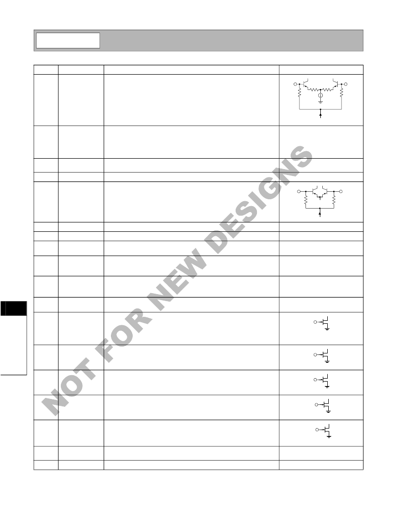
Interface Schematic
2
Q REF
See pin 1.
3
GND 1
4
5
NC
LO IN+
Balanced LO Input Pin. This pin is internally DC biased and should be
DC blocked if connected to a device with a DC level present. For single-
ended input operation, one pin is used as an input and the other LO
The single-ended input impedance is 50
.
6
7
8
LO IN-
NC
VCC1
Same as pin 4, except complementary input.
See pin 5.
This pin is used to supply V
cc
to the modulator circuits. A RF bypass
capacitor should be connected directly to this and ground.
Ground connection. This pin is used for RF ground of the power control
circuitry and the PA driver amplifier. Keep traces physically short and
connect immediately to ground plane for best performance.
This pin is used to supply V
cc
to the power control and pre amp cir-
cuitry. A RF bypass capacitor should be connected directly to this and
ground.
Interstage bias point between pre amp and power amp. This pin should
be pulled up to V
cc
with an 8.2nH inductor for 915MHz.
Analog power control input. This pin can be used as a linear power out-
put control with a range of 20 dB. Maximum output power is achieved
when APC is high. APC is”wire-or’d” with the digital controls, therefore
should be low when using the digital control. The DC input voltage to
the pin should always be less than 3.6V.
This digital power control input sets the medium current and power out-
put, 10mW. It is “wire-or’d” with APC and PC 2 and can be overcome
by either. Therefore, APC and PC 2 must be low to use this setting.
9
GND2
10
VCC2
11
INSTGT
See pin 18.
12
APC
13
PC 1
14
PC 2
This digital power control input set the high current and power output,
100mW. It is “wire-or’d” with APC and PC 1 and can override both of
those controls. Therefore, PC 2 must be low to use other settings.
15
TX PD
Enables all of the IC except for the LO buffer when > 2V.
16
PLLON
Enables the LO buffer amp when > 2V.This can be switched on and off
independently of the rest of the IC. This amp draws 1.5mA typi-
17
18
BIAS
Q REF
Q SIG
BIAS
LO IN-
LO IN+
APC
PC 1
PC 2
TX PD
PLLON
相關PDF資料 |
PDF描述 |
|---|---|
| RF2915 | 433/868/915MHZ FSK/ASK/OOK TRANSCEIVER |
| RF2917 | 433/868/915MHZ FM/FSK RECEIVER |
| RF2919 | 433/868/915MHZ ASK/OOK RECEIVER |
| RF2926 | UHF DUAL CONVERSION TRANSCEIVER |
| RF2938 | 2.4GHZ SPREAD-SPECTRUM TRANSCEIVER |
相關代理商/技術參數(shù) |
參數(shù)描述 |
|---|---|
| RF2915 | 制造商:RFMD 制造商全稱:RF Micro Devices 功能描述:433/868/915MHZ FSK/ASK/OOK TRANSCEIVER |
| RF2917 | 制造商:RFMD 制造商全稱:RF Micro Devices 功能描述:433/868/915MHZ FM/FSK RECEIVER |
| RF2919 | 制造商:RFMD 制造商全稱:RF Micro Devices 功能描述:433/868/915MHZ ASK/OOK RECEIVER |
| RF2926 | 制造商:RFMD 制造商全稱:RF Micro Devices 功能描述:UHF DUAL CONVERSION TRANSCEIVER |
| RF2926-000 | 制造商:TE Connectivity 功能描述:FEMTOSMDC005F-2 - Tape and Reel |
發(fā)布緊急采購,3分鐘左右您將得到回復。