- 您現(xiàn)在的位置:買(mǎi)賣(mài)IC網(wǎng) > PDF目錄385769 > RF2926 (RF MICRO DEVICES INC) UHF DUAL CONVERSION TRANSCEIVER PDF資料下載
參數(shù)資料
| 型號(hào): | RF2926 |
| 廠商: | RF MICRO DEVICES INC |
| 元件分類: | 通信及網(wǎng)絡(luò) |
| 英文描述: | UHF DUAL CONVERSION TRANSCEIVER |
| 中文描述: | SPECIALTY TELECOM CIRCUIT, PQFP48 |
| 封裝: | PLASTIC, LQFP-48 |
| 文件頁(yè)數(shù): | 2/10頁(yè) |
| 文件大?。?/td> | 327K |
| 代理商: | RF2926 |
11-186
RF2926
Rev A5 010404
11
T
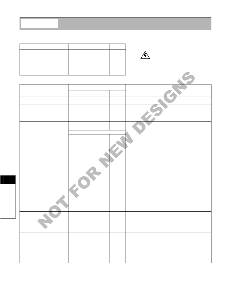
Absolute Maximum Ratings
Parameter
Supply Voltage
Control Voltages
Input RF Level
Output Load VSWR
Operating Ambient Temperature
Storage Temperature
Ratings
-0.5 to +5.5
-0.5 to +5.0
+10
50:1
-40 to +85
-40 to +150
Unit
V
DC
V
DC
dBm
°C
°C
Parameter
Specification
Typ.
Unit
Condition
Min.
Max.
Overall
RF Frequency Range
VCO
VCO Frequency Range
VCO OUT Level
VCO OUT Impedance
Transmit Section
Max Modulation Frequency
Min Modulation Frequency
Maximum Power Level
Power Control Range
Power Control Sensitivity
Max FM Deviation
T=25°C, V
CC
=3.6V, Freq=433MHz
300 to 1000
MHz
300 to 1000
-18
50
MHz
dBm
50
load impedance
2
MHz
Set by loop filter bandwidth
+2
20
TBD
200
dBm
dB
dB/V
kHz
Freq=433MHz
See plot
Instantaneous frequency deviation is
inversely proportional with the modulation
voltage
TX ENABL=“1”
TX ENABL=“0”
TX Mode
Antenna Port Impedance
Antenna Port Impedance
Antenna Port VSWR
Modulation Input Impedance
Harmonics
50
TBD
1.5:1
4
k
dBm
-50
Measured on eval board with RF filters in
system.
Spurious
Overall Receive Section
Frequency Range
RX Sensitivity
RSSI DC Output Range
RSSI Sensitivity
RSSI Dynamic Range
LNA and Mixer
Cascaded Gain
Cascaded Noise Figure
Cascaded Input IP
3
LO Leakage
First IF Section
IF 3dB Bandwidth
Voltage Gain
Noise Figure
Input IP
3
IF1 Input Impedance
IF1 Output Impedance
TBD
dBc
300 to 1000
-99
0.7 to 2.2
25
80
MHz
dBm
V
mV/dB
dB
IF BW=400kHz, Freq=915MHz, S/N=8dB
R
LOAD
=51k
See plot
70
18
7
dB
dB
dBm
dBm
Freq=915MHz; RX current 12mA
Freq=915MHz; RX current 12mA
Freq=915MHz; RX current 12mA
-18.5
-70
130
34
13
TBD
330
330
MHz
dB
dB
mV
PP
IF=110.6MHz, Z
L
=330
Caution!
ESD sensitive device.
RF Micro Devices believes the furnished information is correct and accurate
at the time of this printing. However, RF Micro Devices reserves the right to
make changes to its products without notice. RF Micro Devices does not
assume responsibility for the use of the described product(s).
相關(guān)PDF資料 |
PDF描述 |
|---|---|
| RF2938 | 2.4GHZ SPREAD-SPECTRUM TRANSCEIVER |
| RF2942 | UHF QUADRATURE MODULATOR AND TRANSMITTER |
| RF2945 | 433/868/915MHZ FSK/ASK/OOK TRANSCEIVER |
| RF2958 | 2.4GHz SPREAD-SPECTRUM TRANSCEIVER |
| RF2958PCBA | 2.4GHz SPREAD-SPECTRUM TRANSCEIVER |
相關(guān)代理商/技術(shù)參數(shù) |
參數(shù)描述 |
|---|---|
| RF2926-000 | 制造商:TE Connectivity 功能描述:FEMTOSMDC005F-2 - Tape and Reel |
| RF2926PCBA | 制造商:RFMD 制造商全稱:RF Micro Devices 功能描述:UHF DUAL CONVERSION TRANSCEIVER |
| RF2938 | 制造商:RF Micro Devices Inc 功能描述:Telecommunication IC |
| RF2938TR13 | 制造商:未知廠家 制造商全稱:未知廠家 功能描述:Interface IC |
| RF2942 | 制造商:RFMD 制造商全稱:RF Micro Devices 功能描述:UHF QUADRATURE MODULATOR AND TRANSMITTER |
發(fā)布緊急采購(gòu),3分鐘左右您將得到回復(fù)。