- 您現(xiàn)在的位置:買賣IC網(wǎng) > PDF目錄385770 > RF3404 (RF MICRO DEVICES INC) DUAL-BAND/TRI-MODE CDMA LOW NOISE AMPLIFIER/MIXER MODULE PDF資料下載
參數(shù)資料
| 型號(hào): | RF3404 |
| 廠商: | RF MICRO DEVICES INC |
| 元件分類: | 無繩電話/電話 |
| 英文描述: | DUAL-BAND/TRI-MODE CDMA LOW NOISE AMPLIFIER/MIXER MODULE |
| 中文描述: | TELECOM, CELLULAR, RF AND BASEBAND CIRCUIT, PBGA48 |
| 封裝: | 8 X 8 MM, MODULE, LGA-48 |
| 文件頁數(shù): | 10/12頁 |
| 文件大小: | 202K |
| 代理商: | RF3404 |

Preliminary
8-42
RF3404
Rev A1 010918
8
F
traces required to converge on the perimeter of the
module. Routing is eased by viaholes that can be
placed between the inner row of connections and the
center ground pad in the cellular/PCS telephone PCB.
Why Use Integrated Modules
Decreased Board Area
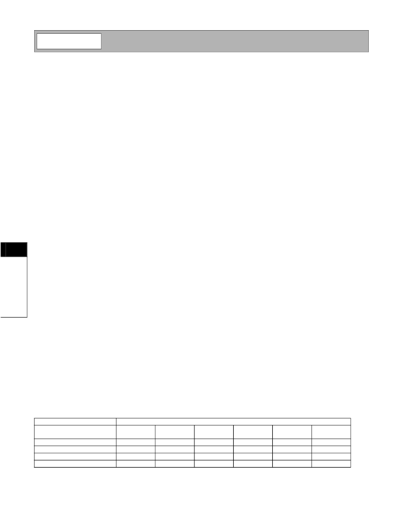
Table A shows a comparison between the leading four
design approaches for dual-band/tri-mode CDMA front
ends:
1. discrete LNAs and discrete mixers with off-chip
matching for each component,
2. single band cellular and PCS LNA/Mixer MMICs
with off-chip matching,
3. single MMIC dual band chips with off-chip matching
and finally
4. fully integrated modules like the RF3404.
Table A summarizes the number of SMD components
for each approach as well as the typical amount of
phone board space required for a complete layout.The
RF3404 represents a 50 percent to 70 percent reduc-
tion in the amount of board space required when com-
pared with the most highly integrated chip solutions on
the market today. Furthermore, it represents the larg-
est percentage improvement in board space savings
for any of the other increased integration gains in
recent years.
Reduced BOM Counts
Another area where one can see marked improvement
is in BOM reduction. The RF3404 reduces the BOM
from the most highly integrated alternatives available
today that contain approximately 25 components to
only three. The three are VCC-bypassing capacitors
that depend on the frequency response of the phone
board power supply and a resistor.
Simplify the Supply Chain
The supply chain can be significantly simplified with
the elimination of two dozen components that would
not need to be source selected, qualified, purchased,
received, stored, coordinated or delivered to the fac-
tory floor.
Decreased Engineering and Product Cycle Time
With a single module solution the RF engineering
required to design the front end is significantly
reduced. The RF3404 module allows for a design-in
solution meeting all of the IS95B requirements, which
requires significantly less engineering.
Decreased Assembly Costs
Accordingly, assembly costs are also reduced. With
SMD placement costs running in the range of 1.0cents
to 1.3cents per placement and with the placement of
die packages, SAWs, and modules costing even more
per placement, one can eliminate somewhere around
35cents from the cost of assembly with modules and
improve factory throughput.
Improve Phone Level Yield
Known good RF performance at the module level is
available with integrated modules that have been RF
tested. Phone level yield can be improved, in addition
to the improvement in yield from placing two dozen
fewer components.
Improved Reliability
Mechanical attachment and reliability is improved with
this module technology due to a variety of factors. The
first is the elimination of numerous components and
thus solder joints, which directly aids overall phone reli-
ability. Another important factor is the matched coeffi-
cient of thermal expansion (CTE) between the laminate
module and the cellular/PCS telephone PCB that elimi-
nates much of the solder stress potential found in low-
temperature-cofired-ceramic
modules and should provide the most robust solution
for the stringent mechanical shock and drop tests that
mobile telephone hardware must survive.
(LTCC)
or
chip-scale
Table A. Comparison of Alternate CDMA Front-End Solution Approaches
Number of Components*
Inductors
Level of Integration
Caps
Resistors
Saws
Total
Components
3
24
35
40
Board Area
(sq. mm)
67
~200
~280
~350
RF3404 Module
Dual Band Integrated MMIC
Single Band Integrated MMIC
LNA/Mixer Discrete Solution
*Does not include IF matching components to IF SAW filters.
2
4
8
8
0
7
6
6
0
2
2
2
11
19
24
相關(guān)PDF資料 |
PDF描述 |
|---|---|
| RF3404PCBA | DUAL-BAND/TRI-MODE CDMA LOW NOISE AMPLIFIER/MIXER MODULE |
| RF3800 | GaAs HBT PRE-DRIVER AMPLIFIER |
| RF3800PCBA-416 | GaAs HBT PRE-DRIVER AMPLIFIER |
| RF3802 | GaAs HBT PRE-DRIVER AMPLIFIER |
| RF3802PCBA-410 | GaAs HBT PRE-DRIVER AMPLIFIER |
相關(guān)代理商/技術(shù)參數(shù) |
參數(shù)描述 |
|---|---|
| RF3404D | 功能描述:信號(hào)調(diào)節(jié) 433.92MHz Narrowband Receiver Front End RoHS:否 制造商:EPCOS 產(chǎn)品:Duplexers 頻率:782 MHz, 751 MHz 頻率范圍: 電壓額定值: 帶寬: 阻抗:50 Ohms 端接類型:SMD/SMT 封裝 / 箱體:2.5 mm x 2 mm 工作溫度范圍:- 30 C to + 85 C 封裝:Reel |
| RF3404E | 功能描述:信號(hào)調(diào)節(jié) 433.92MHz Narrowband Receiver Front End RoHS:否 制造商:EPCOS 產(chǎn)品:Duplexers 頻率:782 MHz, 751 MHz 頻率范圍: 電壓額定值: 帶寬: 阻抗:50 Ohms 端接類型:SMD/SMT 封裝 / 箱體:2.5 mm x 2 mm 工作溫度范圍:- 30 C to + 85 C 封裝:Reel |
| RF3404PCBA | 制造商:RFMD 制造商全稱:RF Micro Devices 功能描述:DUAL-BAND/TRI-MODE CDMA LOW NOISE AMPLIFIER/MIXER MODULE |
| RF341-12 | 制造商:Teledyne Relays 功能描述:RELAY - Bulk |
| RF341-26 | 制造商:TELEDYNE 制造商全稱:TELEDYNE 功能描述:ULTRAMINIATURE MAGNETIC LATCHING TO-5 RELAYS SPDT DC TO C BAND |
發(fā)布緊急采購,3分鐘左右您將得到回復(fù)。