- 您現(xiàn)在的位置:買賣IC網(wǎng) > PDF目錄368604 > RV2207N (Raytheon Company) Voltage Controlled Oscillator PDF資料下載
參數(shù)資料
| 型號(hào): | RV2207N |
| 廠商: | Raytheon Company |
| 英文描述: | Voltage Controlled Oscillator |
| 中文描述: | 壓控振蕩器 |
| 文件頁(yè)數(shù): | 2/12頁(yè) |
| 文件大小: | 74K |
| 代理商: | RV2207N |
RC2207
PRODUCT SPECIFICATION
2
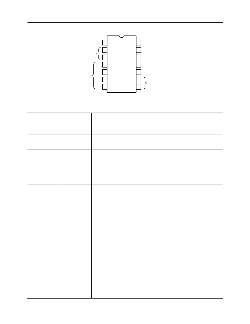
Pin Assignments
Pin Descriptions
Pin Name
Bias for Single
Supply
Pin Number
11
Pin Function Description
For single supply operations, pin 11 should be externally biased to a
potential between +V
S
/3 and +V
S
/2 (see Figure 8). The bias current at pin
11 is nominally 5% of the total oscillation timing current I
The internal impedance at these pins is approximately 5 k
are <1.4V for zero and > 3V for one logic levels referenced to the DC voltage
at pin 10.
For split supply operation, this pin serves as circuit ground. For single supply
operation, pin 10 should be AC grounded through a 1
During split supply operation, a ground current of 2 I
terminal, where I
T
is the total timing current.
The squarewave output at pin 13 is an open-collector stage capable of
sinking up to 20 mA of load current. R
this output. Recommended values for R
The RC2207 is designed to operate over a power supply range of +4V to
±
13V for split supplies, or 8V to 26V for single supplies. At high supply
voltages, the frequency sweep range is reduced. Performance is optimum
for
±
6V, or 12V single supply operation.
The oscillator frequency is inversely proportional to the timing capacitor, C.
The minimum capacitance value is limited by stray capacitances and the
maximum value by physical size and leakage current considerations.
Recommended values range from 100 pF to 100
be non-polarized.
The timing resistors determine the total timing current, I
charge the timing capacitor. Values for timing resistors can range from 1.5
k
to 2 M
; however, for optimum temperature and power supply stability,
recommended values are 4 k
to 200 k
resistor leads should be kept as short as possible. For noise environments,
unused or deactivated timing terminals should be bypassed to ground
through 0.1
μ
F capacitors. Otherwise, they may be left open.
The output at pin 14 is a trianglewave with a peak swing of approximately
one-half of the total supply voltage. Pin 14 has a very low output impedance
of 10
and is internally protected against short circuits.
T
.
Binary Keying
Inputs
8, 9
. Keying levels
Ground
10
μ
flows out of this
F bypass capacitor.
T
Squarewave
Output
13
L
serves as a pull-up load resistor for
L
range from 1 k
to 10 k
Supply Voltage
(+V
S
, –V
S
)
1, 12
Timing Capacitor
2, 3
μ
F. The capacitor should
Timing Resistors
(R1–R4)
4–7
T
, available to
. To avoid parasitic pick up, timing
Trianglewave
Output
14
Notice that the triangle waveform linearity is sensitive to parasite coupling
between the square and the trianglewave outputs (pins 13 and 14). In board
layout or circuit wiring, care should be taken to minimize stray wiring
capacitance between those pins.
1
2
3
4
5
6
7
14
13
12
11
10
9
8
65-2207-02
Binary
Keying
Inputs
GND
Bias
Squarewave Output
Trianglewave Output
+V
S
Timing
Capacitor
Timing
Resistors
R1
R2
R3
R4
+V
S
相關(guān)PDF資料 |
PDF描述 |
|---|---|
| RV4190N | RADIATION HARDENED HIGH EFFICIENCY, 5 AMP SWITCHING REGULATORS |
| RV8564C2 | Real Time clock |
| RX-0912S | 1 Watt SIP7 & DIP14 Single & Dual Output |
| RX-0505S | 1 Watt SIP7 & DIP14 Single & Dual Output |
| RX-0509S | 1 Watt SIP7 & DIP14 Single & Dual Output |
相關(guān)代理商/技術(shù)參數(shù) |
參數(shù)描述 |
|---|---|
| RV2211AM | 制造商:未知廠家 制造商全稱:未知廠家 功能描述:ASK/FSK Demodulator |
| RV2211AN | 制造商:未知廠家 制造商全稱:未知廠家 功能描述:ASK/FSK Demodulator |
| RV2211N | 制造商:未知廠家 制造商全稱:未知廠家 功能描述:FSK Demodulator/Tone Decoder |
| RV2220M0JTR-0405 | 制造商:LELON ELECTRONICS CORP. 功能描述: |
| RV2-25V100M-R | 功能描述:鋁質(zhì)電解電容器-SMD 25V 10uF RoHS:否 制造商:Vishay/BC Components 電容:2200 uF 容差:20 % 電壓額定值:16 V ESR: 工作溫度范圍:- 55 C to + 150 C 尺寸:16 mm W x 16 mm L x 21 mm H 產(chǎn)品:High Temp Electrolytic Capacitors |
發(fā)布緊急采購(gòu),3分鐘左右您將得到回復(fù)。