- 您現(xiàn)在的位置:買賣IC網(wǎng) > PDF目錄192295 > S25FL004D0LMFI011 (SPANSION LLC) 4 Megabit CMOS 3.0 Volt Flash Memory with 50 Mhz SPI Bus Interface PDF資料下載
參數(shù)資料
| 型號: | S25FL004D0LMFI011 |
| 廠商: | SPANSION LLC |
| 元件分類: | PROM |
| 英文描述: | 4 Megabit CMOS 3.0 Volt Flash Memory with 50 Mhz SPI Bus Interface |
| 中文描述: | 4M X 1 FLASH 3V PROM, PDSO8 |
| 封裝: | 0.208 INCH, LEAD FREE, SOP-8 |
| 文件頁數(shù): | 17/36頁 |
| 文件大小: | 724K |
| 代理商: | S25FL004D0LMFI011 |
第1頁第2頁第3頁第4頁第5頁第6頁第7頁第8頁第9頁第10頁第11頁第12頁第13頁第14頁第15頁第16頁當(dāng)前第17頁第18頁第19頁第20頁第21頁第22頁第23頁第24頁第25頁第26頁第27頁第28頁第29頁第30頁第31頁第32頁第33頁第34頁第35頁第36頁
24
S25FL Family (Serial Peripheral Interface) S25FL004D
S25FL004D_00A0 June 28, 2004
Ad va n c e
In f o rm a t i o n
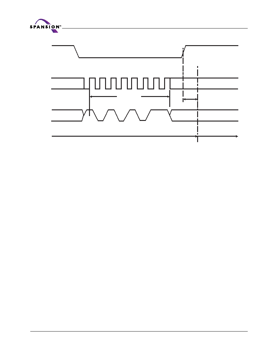
Figure 15. Release from Deep Power Down Instruction Sequence
Release from Deep Power Down and Read Electronic Signature (RES)
Once the device has entered Deep Power Down mode, all instructions are ignored
except the RES instruction. The RES instruction can also be used to read the 8-
bit Electronic Signature of the device on the SO pin. The RES instruction always
provides access to the Electronic Signature of the device (except while an Erase,
Program or WRSR cycle is in progress), and can be applied even if DP mode has
not been entered. Any RES instruction executed while an Erase, Program or
WRSR cycle is in progress is not decoded, and has no effect on the cycle in
progress.
The device features an 8-bit Electronic Signature, whose value for the S25FL004D
is 12h. This can be read using RES instruction.
The device is first selected by driving Chip Select (CS#) Low. The instruction code
is followed by 3 dummy bytes, each bit being latched-in on Serial Data Input (SI)
during the rising edge of Serial Clock (SCK). Then, the 8-bit Electronic Signature,
stored in the memory, is shifted out on Serial Data Output (SO), each bit being
shifted out during the falling edge of Serial Clock (SCK).
The instruction sequence is shown in Figure 16.
The Release from Deep Power Down and Read Electronic Signature (RES) is ter-
minated by driving Chip Select (CS#) High after the Electronic Signature has
been read at least once. Sending additional clock cycles on Serial Clock (SCK),
while Chip Select (CS#) is driven Low, causes the Electronic Signature to be out-
put repeatedly.
When Chip Select is driven High, the device is put in the Stand-by Power mode.
If the device was not previously in the Deep Power Down mode, the transition to
the Stand-by Power mode is immediate. If the device was previously in the Deep
Power Down mode, though, the transition to the Standby mode is delayed by
tRES, and Chip Select (CS#) must remain High for at lease tRES(max), as specified
in Table 8. Once in the Stand-by Power mode, the device waits to be selected, so
that it can receive, decode and execute instructions.
CS#
SCK
SI
0
1
23
4
5
6
7
Instruction
Deep Power Down Mode
t
RES
Standby Mode
相關(guān)PDF資料 |
PDF描述 |
|---|---|
| S25FL004D0LMFI013 | 4 Megabit CMOS 3.0 Volt Flash Memory with 50 Mhz SPI Bus Interface |
| S25FL004D0LNFI011 | 4 Megabit CMOS 3.0 Volt Flash Memory with 50 Mhz SPI Bus Interface |
| S25FL004D0LNFI013 | 4 Megabit CMOS 3.0 Volt Flash Memory with 50 Mhz SPI Bus Interface |
| S25FL004D | 4 Megabit CMOS 3.0 Volt Flash Memory with 50 Mhz SPI Bus Interface |
| S25FL004D0LNAI011 | 4 Megabit CMOS 3.0 Volt Flash Memory with 50 Mhz SPI Bus Interface |
相關(guān)代理商/技術(shù)參數(shù) |
參數(shù)描述 |
|---|---|
| S25FL004D0LMFI013 | 制造商:SPANSION 制造商全稱:SPANSION 功能描述:4 Megabit CMOS 3.0 Volt Flash Memory with 50 Mhz SPI Bus Interface |
| S25FL004D0LNAI011 | 制造商:SPANSION 制造商全稱:SPANSION 功能描述:4 Megabit CMOS 3.0 Volt Flash Memory with 50 Mhz SPI Bus Interface |
| S25FL004D0LNAI013 | 制造商:SPANSION 制造商全稱:SPANSION 功能描述:4 Megabit CMOS 3.0 Volt Flash Memory with 50 Mhz SPI Bus Interface |
| S25FL004D0LNFI011 | 制造商:SPANSION 制造商全稱:SPANSION 功能描述:4 Megabit CMOS 3.0 Volt Flash Memory with 50 Mhz SPI Bus Interface |
| S25FL004D0LNFI013 | 制造商:SPANSION 制造商全稱:SPANSION 功能描述:4 Megabit CMOS 3.0 Volt Flash Memory with 50 Mhz SPI Bus Interface |
發(fā)布緊急采購,3分鐘左右您將得到回復(fù)。