- 您現(xiàn)在的位置:買賣IC網(wǎng) > PDF目錄192297 > S29GL032M10TAIR00 (SPANSION LLC) MirrorBit Flash Family PDF資料下載
參數(shù)資料
| 型號(hào): | S29GL032M10TAIR00 |
| 廠商: | SPANSION LLC |
| 元件分類: | PROM |
| 英文描述: | MirrorBit Flash Family |
| 中文描述: | 4M X 8 FLASH 3V PROM, 100 ns, PDSO40 |
| 封裝: | MO-142CD, TSOP-40 |
| 文件頁(yè)數(shù): | 82/116頁(yè) |
| 文件大?。?/td> | 6024K |
| 代理商: | S29GL032M10TAIR00 |
第1頁(yè)第2頁(yè)第3頁(yè)第4頁(yè)第5頁(yè)第6頁(yè)第7頁(yè)第8頁(yè)第9頁(yè)第10頁(yè)第11頁(yè)第12頁(yè)第13頁(yè)第14頁(yè)第15頁(yè)第16頁(yè)第17頁(yè)第18頁(yè)第19頁(yè)第20頁(yè)第21頁(yè)第22頁(yè)第23頁(yè)第24頁(yè)第25頁(yè)第26頁(yè)第27頁(yè)第28頁(yè)第29頁(yè)第30頁(yè)第31頁(yè)第32頁(yè)第33頁(yè)第34頁(yè)第35頁(yè)第36頁(yè)第37頁(yè)第38頁(yè)第39頁(yè)第40頁(yè)第41頁(yè)第42頁(yè)第43頁(yè)第44頁(yè)第45頁(yè)第46頁(yè)第47頁(yè)第48頁(yè)第49頁(yè)第50頁(yè)第51頁(yè)第52頁(yè)第53頁(yè)第54頁(yè)第55頁(yè)第56頁(yè)第57頁(yè)第58頁(yè)第59頁(yè)第60頁(yè)第61頁(yè)第62頁(yè)第63頁(yè)第64頁(yè)第65頁(yè)第66頁(yè)第67頁(yè)第68頁(yè)第69頁(yè)第70頁(yè)第71頁(yè)第72頁(yè)第73頁(yè)第74頁(yè)第75頁(yè)第76頁(yè)第77頁(yè)第78頁(yè)第79頁(yè)第80頁(yè)第81頁(yè)當(dāng)前第82頁(yè)第83頁(yè)第84頁(yè)第85頁(yè)第86頁(yè)第87頁(yè)第88頁(yè)第89頁(yè)第90頁(yè)第91頁(yè)第92頁(yè)第93頁(yè)第94頁(yè)第95頁(yè)第96頁(yè)第97頁(yè)第98頁(yè)第99頁(yè)第100頁(yè)第101頁(yè)第102頁(yè)第103頁(yè)第104頁(yè)第105頁(yè)第106頁(yè)第107頁(yè)第108頁(yè)第109頁(yè)第110頁(yè)第111頁(yè)第112頁(yè)第113頁(yè)第114頁(yè)第115頁(yè)第116頁(yè)
66
S29GL-M MirrorBitTM Flash Family
S29GL-M_00_B8 February 7, 2007
Data
Sheet
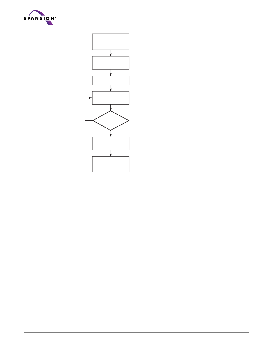
Figure 5. Program Suspend/Program Resume
Chip Erase Command Sequence
Chip erase is a six bus cycle operation. The chip erase command sequence is initiated by writing
two unlock cycles, followed by a set-up command. Two additional unlock write cycles are then
followed by the chip erase command, which in turn invokes the Embedded Erase algorithm. The
device does not require the system to preprogram prior to erase. The Embedded Erase algorithm
automatically preprograms and verifies the entire memory for an all zero data pattern prior to
electrical erase. The system is not required to provide any controls or timings during these oper-
command sequence.
When the Embedded Erase algorithm is complete, the device returns to the read mode and ad-
dresses are no longer latched. The system can determine the status of the erase operation by
using DQ7, DQ6, or DQ2. See Write Operation Status for information on these status bits.
Any commands written during the chip erase operation are ignored. However, note that a hard-
ware reset immediately terminates the erase operation. If that occurs, the chip erase command
sequence should be reinitiated once the device returns to reading array data, to ensure data
integrity.
Figure 6 illustrates the algorithm for the erase operation. See Erase and Programming Perfor-
Sector Erase Command Sequence
Sector erase is a six bus cycle operation. The sector erase command sequence is initiated by writ-
ing two unlock cycles, followed by a set-up command. Two additional unlock cycles are written,
and are then followed by the address of the sector to be erased, and the sector erase command.
sequence.
Program Operation
or Write-to-Buffer
Sequence in Progress
Write Program Suspend
Command Sequence
Command is also valid for
Erase-suspended-program
operations
Autoselect and SecSi Sector
read operations are also allowed
Data cannot be read from erase- or
program-suspended sectors
Write Program Resume
Command Sequence
Read data as
required
Done
reading?
No
Yes
Write address/data
XXXh/30h
Device reverts to
operation prior to
Program Suspend
Write address/data
XXXh/B0h
Wait 15
μs
相關(guān)PDF資料 |
PDF描述 |
|---|---|
| S29GL032M10TAIR03 | MirrorBit Flash Family |
| S29GL032M10TAIR10 | MirrorBit Flash Family |
| S29GL032M10TAIR13 | MirrorBit Flash Family |
| S29GL032M10TAIR20 | MirrorBit Flash Family |
| S29GL032M10TAIR23 | Conductive Polymer Chip Capacitors / T530 Series - High Capacitance/Ultra-Low ESR; Capacitance [nom]: 680uF; Working Voltage (Vdc)[max]: 4V; Capacitance Tolerance: +/-20%; Dielectric: Conductive Polymer; ESR: 5.0mΩ; Lead Style: Surface-Mount Chip; Lead Dimensions: 7343-40; Termination: Solder Coated (SnPb, Pb 5% min); Body Dimensions: 7.3mm x 4.3mm x 4mm; Temperature Range: -55C to +125C; Container: Tape & Reel; Qty per Container: 500; Features: High Capacitance; Ultra-Low ESR |
相關(guān)代理商/技術(shù)參數(shù) |
參數(shù)描述 |
|---|---|
| S29GL032M10TAIR02 | 制造商:SPANSION 制造商全稱:SPANSION 功能描述:MirrorBit Flash Family |
| S29GL032M10TAIR03 | 制造商:SPANSION 制造商全稱:SPANSION 功能描述:MirrorBit Flash Family |
| S29GL032M10TAIR10 | 制造商:SPANSION 制造商全稱:SPANSION 功能描述:MirrorBit Flash Family |
| S29GL032M10TAIR12 | 制造商:SPANSION 制造商全稱:SPANSION 功能描述:MirrorBit Flash Family |
| S29GL032M10TAIR13 | 制造商:SPANSION 制造商全稱:SPANSION 功能描述:MirrorBit Flash Family |
發(fā)布緊急采購(gòu),3分鐘左右您將得到回復(fù)。