- 您現(xiàn)在的位置:買賣IC網(wǎng) > PDF目錄373347 > S3270 (Electronic Theatre Controls, Inc.) POSITION SENSITIVE DETECTOR PDF資料下載
參數(shù)資料
| 型號(hào): | S3270 |
| 廠商: | Electronic Theatre Controls, Inc. |
| 英文描述: | POSITION SENSITIVE DETECTOR |
| 中文描述: | 位置靈敏探測器 |
| 文件頁數(shù): | 13/16頁 |
| 文件大小: | 1289K |
| 代理商: | S3270 |
10
Figure 6-1 Response wavelength example of PSD
KPSDC0078EB
2) Diffusion time t
2
of carriers generated outside the deple-
tion layer
Carriers are also generated outside the depletion layer
when light is absorbed in the PSD chip surrounding areas
outside the active area or at locations deeper than the de-
pletion layer in the substrate. These carriers diffuse through
the substrate and are extracted as an output. The time t
2
required for these carriers to diffuse may be more than sev-
eral microseconds.
The equation below gives the approximate rise time tr of a
PSD. Figure 6-1 shows typical output waveforms in re-
sponse to stepped light input.
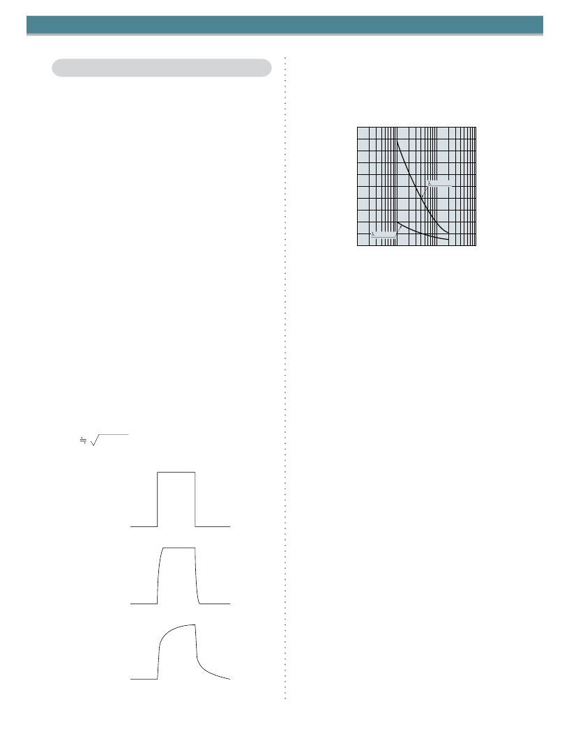
Figure 6-2 shows the relation between the rise time and re-
verse voltage measured at different wavelengths. The rise
time can be reduced by increasing the reverse voltage and
using a light beam of shorter wavelengths. Selecting a PSD
with a small Rie is also effective in improving the rise time.
Figure 6-2 Rise time vs. reverse voltage (S4583-06)
A method for integrating position signals can be used when
detecting pulsed light having a pulse width shorter than the
PSD rise time.
Characteristic and use
6. Response speed
As with photodiodes, the response speed of PSD is the
time required for the generated carriers to be extracted as
current by an external circuit. This is generally expressed
as the rise time tr and is an important parameter when de-
tecting a spot light traveling over the active surface at high
speeds or using pulse-modulated light for subtracting the
background light. The rise time is defined as the time need-
ed for the output signal to rise from 10 to 90 % of its peak
value and is chiefly determined by the following two factors.
1) Time constant t
1
determined by the interelectrode resist-
ance, load resistance and terminal capacitance
The interelectrode resistance Rie of PSD basically acts as
load resistance R
L
, so the time constant t
1
is given by the
interelectrode resistance Rie and terminal capacitance Ct,
as follows:
t
1
= 2.2 . Ct . (Rie + R
L
) ......... (6-1)
The rise time listed in our PSD datasheets is measured
with a spot light striking the center of the active area with
the interelectrode resistance Rie distributed between the
electrodes. So the time constant t
1
is as follows:
t
1
= 0.5 . Ct . (Rie + R
L
) ......... (6-2)
KPSDB0110EA
REVERSE VOLTAGE (V)
(Typ. Ta=25
C)
R
1
0.1
0
10
8
6
4
2
10
100
l
=890 nm
l
=650 nm
t
12
+ t
22
.................... (6-3)
tr
LIGHT INPUT
OUTPUT WAVEFORM
(t
1
>>t
2
)
OUTPUT WAVEFORM
(t
2
>>t
1
)
相關(guān)PDF資料 |
PDF描述 |
|---|---|
| S3271-05 | POSITION SENSITIVE DETECTOR |
| S3272-05 | POSITION SENSITIVE DETECTOR |
| S3273-05 | POSITION SENSITIVE DETECTOR |
| S3932 | POSITION SENSITIVE DETECTOR |
| S3979 | POSITION SENSITIVE DETECTOR |
相關(guān)代理商/技術(shù)參數(shù) |
參數(shù)描述 |
|---|---|
| S327-06 | 功能描述:電路板硬件 - PCB 5MM FUSE CLIP 1K BAG RoHS:否 制造商:Harwin 類型:Shield Clip 長度:9.4 mm 螺紋大小: 外徑: 材料:Beryllium Copper 電鍍:Tin |
| S3271-05 | 制造商:未知廠家 制造商全稱:未知廠家 功能描述:POSITION SENSITIVE DETECTOR |
| S3272-05 | 制造商:未知廠家 制造商全稱:未知廠家 功能描述:POSITION SENSITIVE DETECTOR |
| S3273-05 | 制造商:未知廠家 制造商全稱:未知廠家 功能描述:POSITION SENSITIVE DETECTOR |
| S3274 | 制造商:MERKLE-KORFF INDUSTRIES 功能描述:Old Colman P/N: 97.331.0097 |
發(fā)布緊急采購,3分鐘左右您將得到回復(fù)。