- 您現(xiàn)在的位置:買賣IC網(wǎng) > PDF目錄373347 > S3273-05 (Electronic Theatre Controls, Inc.) POSITION SENSITIVE DETECTOR PDF資料下載
參數(shù)資料
| 型號: | S3273-05 |
| 廠商: | Electronic Theatre Controls, Inc. |
| 英文描述: | POSITION SENSITIVE DETECTOR |
| 中文描述: | 位置靈敏探測器 |
| 文件頁數(shù): | 8/16頁 |
| 文件大小: | 1289K |
| 代理商: | S3273-05 |
5
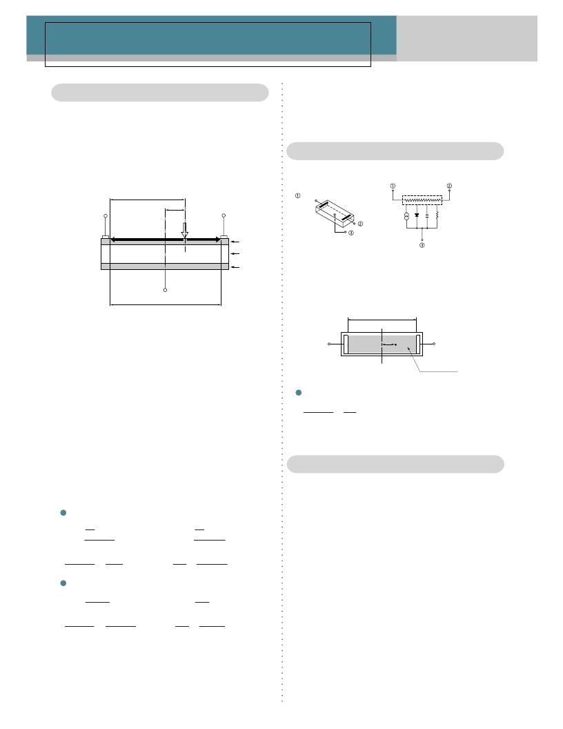
A PSD basically consists of a uniform resistive layer
formed on one or both surfaces of a high-resistivity semi-
conductor substrate, and a pair of electrodes formed on
both ends of the resistive layer for extracting position
signals. The active area, which is also a resistive layer,
has a PN junction that generates photocurrent by means
of the photovoltaic effect.
KPSDC0010EA
KPSDC0006EA
By finding the difference or ratio of Ix
1
to Ix
2
, the light input
position can be obtained by the formulas (1-3), (1-4), (1-7)
and (1-8) irrespective of the incident light intensity level
and its changes. The light input position obtained here cor-
responds to the center-of-gravity of the light beam.
Figure 1-1 shows a sectional view of a PSD using a simple
illustration to explain the operating principle. The PSD has
a P-type resistive layer formed on an N-type high-resistive
silicon substrate. This P-layer serves as an active area for
photoelectric conversion and a pair of output electrodes
are formed on the both ends of the P-layer. On the
backside of the silicon substrate is an N-layer to which a
common electrode is connected. Basically, this is the
same structure as that of PIN photodiodes except for the
P-type resistive layer on the surface.
When a spot light strikes the PSD, an electric charge
proportional to the light intensity is generated at the
incident position. This electric charge is driven through the
resistive layer and collected by the output electrodes X
1
and X
2
as photocurrents, while being divided in inverse
proportion to the distance between the incident position
and each electrode.
The relation between the incident light position and the
photocurrents from the output electrodes X
1
, X
2
is given by
the following formulas.
l
When the center point of PSD is set at the origin:
L
X
2
L
X
l
When the end of PSD is set at the origin:
B
L
X
Io : Total photocurrent (I
X1
+ I
X2
)
I
X1
: Output current from electrode X
1
I
X2
: Output current from electrode X
2
L
X
: Resistance length (length of the active area)
X
A
:
Distance from the electrical center of PSD to the light input position
X
B
:
Distance from the electrode X
1
to the light input position
In the above formula, I
X1
and I
X2
are the output currents
obtained from the electrodes shown in Figure 2-2.
l
Position conversion formula (See Figure 2-2.)
Two-dimensional PSDs are grouped by structure into duo-
lateral and tetra-lateral types. Among the tetra-lateral type
PSDs, a pin-cushion type with an improved active area
and electrodes is also provided. (See
“
3-3
”
.) The position
conversion formulas slightly differ according to the PSD
structure. Two-dimensional PSDs have two pairs of output
electrodes, X
1
, X
2
and Y
1
, Y
2
.
3-1 Duo-lateral type PSD
On the duo-lateral type, the N-layer shown in the sectional
view of Figure 1-1 is processed to form a resistive layer,
and two pair of electrodes are formed on both surfaces as
X and Y electrodes arranged at right angles. (See Figure
3-1.) The X position signals are extracted from the X elec-
trodes on the upper surface, while the Y position signals
are extracted from the Y electrodes on the bottom surface.
As shown in Figure 3-1, a photocurrent with a polarity op-
posite that of the other surface is on each surface, to pro-
duce signal currents twice as large as the tetra-lateral type
and achieve a higher position resolution. In addition, when
compared to the tetra-lateral type, the duo-lateral type of-
fers excellent position detection characteristics because
the electrodes are not in close proximity. The light input
position can be calculated from conversion formulas (3-1)
and (3-2).
Figure 2-1 Structure chart, equivalent circuit (one-dimensional PSD)
Figure 2-2
Active area chart (one-dimensional PSD)
L
X
KPSDC0005EA
Figure 1-1 PSD sectional view
I
X2
=
= X
L
X
I
X2
-
I
X1
I
X1
+
I
X2
A
= X
L
X
+ 2
X
A
I
X1
I
X2
A
= X
L
X
I
X2
-
I
X1
I
X1
+
I
X2
B
- L
X
= ........ (2-1)
L
X
I
X2
- I
X1
I
X1
+ I
X2
= X
X
B
I
X1
I
X2
B
I
X1
= X
I
X2
= X
L
X
B
Characteristic and use
1.
Basic principle
2. One-dimensional PSD
3. Two-dimensional PSD
I
X1
=
......... (1-1)
×
Io
- X
A
L
X
2
L
X
...... (1-2)
×
Io
+ X
A
OUTPUT I
X1
PHOTOCURRENT
X
B
INCIDENT
LIGHT
P LAYER
RESISTANCE LENGTH L
X
COMMON
ELECTRODE
X
A
OUTPUT I
X2
ELECTRODE X
1
ELECTRODE X
2
I LAYER
N LAYER
X
1
X
2
ACTIVE AREA
x
P
D
Cj
Rsh
Rp
: CURRENT GENERATOR
: IDEAL DIODE
: JUNCTION CAPACITANCE
: SHUNT RESISTANCE
: POSITIONING RESISTANCE
P
D
Cj Rsh
Rp
CATHODE
(COMMON)
ANODE (X
2
)
ANODE (X
1
)
相關(guān)PDF資料 |
PDF描述 |
|---|---|
| S3932 | POSITION SENSITIVE DETECTOR |
| S3979 | POSITION SENSITIVE DETECTOR |
| S3274-05 | POSITION SENSITIVE DETECTOR |
| S393P | Dual Voltage Comparator |
| S393 | Dual Voltage Comparator |
相關(guān)代理商/技術(shù)參數(shù) |
參數(shù)描述 |
|---|---|
| S3274 | 制造商:MERKLE-KORFF INDUSTRIES 功能描述:Old Colman P/N: 97.331.0097 |
| S3274-05 | 制造商:未知廠家 制造商全稱:未知廠家 功能描述:POSITION SENSITIVE DETECTOR |
| S32768 | 制造商:未知廠家 制造商全稱:未知廠家 功能描述:Ultrasonic Sonar Ranging IC |
| S3279-2222-2.00-34 | 制造商:Sunbank (Meggitt) 功能描述:ACCESSORY |
| S327AB | 制造商:CINCH 功能描述:_ |
發(fā)布緊急采購,3分鐘左右您將得到回復(fù)。