- 您現(xiàn)在的位置:買賣IC網(wǎng) > PDF目錄368612 > S6A0031 (SAMSUNG SEMICONDUCTOR CO. LTD.) 8 COM / 80 SEG DRIVER & CONTROLLER FOR STN LCD PDF資料下載
參數(shù)資料
| 型號: | S6A0031 |
| 廠商: | SAMSUNG SEMICONDUCTOR CO. LTD. |
| 英文描述: | 8 COM / 80 SEG DRIVER & CONTROLLER FOR STN LCD |
| 中文描述: | 8的COM / 80賽格驅(qū)動(dòng) |
| 文件頁數(shù): | 21/37頁 |
| 文件大小: | 339K |
| 代理商: | S6A0031 |
第1頁第2頁第3頁第4頁第5頁第6頁第7頁第8頁第9頁第10頁第11頁第12頁第13頁第14頁第15頁第16頁第17頁第18頁第19頁第20頁當(dāng)前第21頁第22頁第23頁第24頁第25頁第26頁第27頁第28頁第29頁第30頁第31頁第32頁第33頁第34頁第35頁第36頁第37頁
8 COM / 80 SEG DRIVER & CONTROLLER FOR STN LCD PRELIMINARY SPEC. VER. 0.5
S6A0031
17
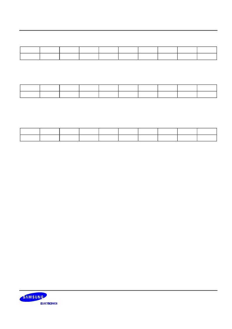
Read Busy Flag and Address
RS
R/W
DB7
DB6
DB5
DB4
DB3
DB2
DB1
DB0
0
1
BF
-
-
A4
A3
A2
A1
A0
This instruction shows whether S6A0031 is in internal operation or not. If the resultant BF is "High", it means the
internal operation is in progress and you have to wait until BF to be "Low", and then the next instruction can be
performed. In this instruction you can read also the value of address counter.
Write Data
RS
R/W
DB7
DB6
DB5
DB4
DB3
DB2
DB1
DB0
1
0
D7
D6
D5
D4
D3
D2
D1
D0
Write binary 8- / 5- bit data to DDRAM / CGRAM
The selection of RAM from DDRAM / CGRAM is set by the previous address set instruction (DDRAM address set,
CGRAM address set). After write operation, the address is automatically increased / decreased by 1, according to
the entry mode.
Read Data
RS
R/W
DB7
DB6
DB5
DB4
DB3
DB2
DB1
DB0
1
1
D7
D6
D5
D4
D3
D2
D1
D0
Read binary 8- / 5- bit data from DDRAM / CGRAM
The selection of RAM is set by the previous address set instruction. If address set instruction of RAM is not
performed before this instruction, the data that read first is invalid, because the direction of AC is not determined. If
you read RAM data several times without RAM address set instruction before read operation, you can get correct
RAM data from the second, and the first data would be incorrect, because there is no time margin to transfer RAM
data. In case of DDRAM read operation, cursor shift instruction plays the same role as DDRAM address set
instruction: it also transfers RAM data to output data register.
After read operation address counter is automatically increased / decreased by 1 according to the entry mode. After
CGRAM read operation, display shift may not be executed correctly.
* In case of RAM write operation, after this operation, AC is increased / decreased by 1 like read operation. In this
time, AC indicates the next address position, but you can read only the previous data by read instruction. RAM
address is dummy data, so the correct RAM data come from the second read transaction. After reading operation,
the address is increased by 1 automatically.
相關(guān)PDF資料 |
PDF描述 |
|---|---|
| S6A0032 | 16 COM / 80 SEG DRIVER & CONTROLLER FOR STN LCD |
| S6A0035 | 53 SEGMENT STATIC DRIVER |
| S6A0065 | 40 CH SEGMENT/COMMON DRIVER FOR DOT MATRIX LCD |
| S6A0069 | 40 SEG / 16 COM DRIVER & CONTROLLER FOR DOT MATRIX LCD |
| S6A0070 | 80 SEG / 16 COM DRIVER & CONTROLLER FOR DOT MATRIX LCD |
相關(guān)代理商/技術(shù)參數(shù) |
參數(shù)描述 |
|---|---|
| S6A0032 | 制造商:SAMSUNG 制造商全稱:Samsung semiconductor 功能描述:16 COM / 80 SEG DRIVER & CONTROLLER FOR STN LCD |
| S6A0035 | 制造商:SAMSUNG 制造商全稱:Samsung semiconductor 功能描述:53 SEGMENT STATIC DRIVER |
| S6A0065 | 制造商:SAMSUNG 制造商全稱:Samsung semiconductor 功能描述:40 CH SEGMENT/COMMON DRIVER FOR DOT MATRIX LCD |
| S6A0065B01-Q08J | 制造商:Samsung Semiconductor 功能描述: |
| S6A0065B01-Q0RJ | 制造商:Samsung Semiconductor 功能描述:N/A - Trays |
發(fā)布緊急采購,3分鐘左右您將得到回復(fù)。