- 您現(xiàn)在的位置:買賣IC網(wǎng) > PDF目錄368613 > S6B33B0A (SAMSUNG SEMICONDUCTOR CO. LTD.) CONNECTOR ACCESSORY PDF資料下載
參數(shù)資料
| 型號: | S6B33B0A |
| 廠商: | SAMSUNG SEMICONDUCTOR CO. LTD. |
| 英文描述: | CONNECTOR ACCESSORY |
| 中文描述: | 連接器附件 |
| 文件頁數(shù): | 21/76頁 |
| 文件大小: | 423K |
| 代理商: | S6B33B0A |
第1頁第2頁第3頁第4頁第5頁第6頁第7頁第8頁第9頁第10頁第11頁第12頁第13頁第14頁第15頁第16頁第17頁第18頁第19頁第20頁當前第21頁第22頁第23頁第24頁第25頁第26頁第27頁第28頁第29頁第30頁第31頁第32頁第33頁第34頁第35頁第36頁第37頁第38頁第39頁第40頁第41頁第42頁第43頁第44頁第45頁第46頁第47頁第48頁第49頁第50頁第51頁第52頁第53頁第54頁第55頁第56頁第57頁第58頁第59頁第60頁第61頁第62頁第63頁第64頁第65頁第66頁第67頁第68頁第69頁第70頁第71頁第72頁第73頁第74頁第75頁第76頁
S6B33B0A PRELIMINARY VER 1.1 144 RGB SEGMENT & 177 COMMON DRIVER FOR 65,536 COLOR STN LCD
17
Serial Interface(PS=”L”)
Communication with the microprocessor occurs via a clock-synchronized serial peripheral interface when PS is low.
When using the serial interface, read operations are not allowed. When the chip select inputs are valid (CS1B = “ L”
& CS2 = “ H”), the serial data is sent most significant bit first on the rising edge of a serial clock going into DB6 and
processed as 8 bit parallel data on the eighth clock. Since the clock signal is easy to be affected by the external
noise caused by the line length, the operation check on the actual machine is recommended. And Invalid, the
internal shift register and the counter are reset.
The serial interface type is selected by setting PS as shown in Table12.
Table 12. Microprocessor Selection for Serial Interface
PS
MPU[1]
CS1B
CS2
D/I
Serial Data
Serial Clock
SPI Mode
L
CS1B
CS2
By S/W
3-Pin
L
H
CS1B
CS2
D/I
DB[7]
DB[6]
4-Pin
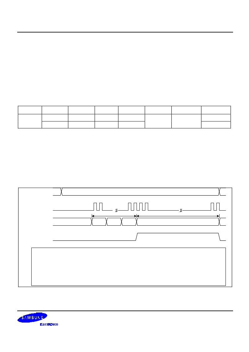
3-Pin SPI Interface (PS = "L" & MPU[1] = "L")
In 3-Pin SPI Interface mode, the pre-defined instruction called Display Data Length is used to indicate whether serial
data input is display or instruction data instead of D/I pin. The data is handled as instruction data until the Display
Data Length instruction is issued. This Display Data Length instruction consists of three bytes instruction. The first
byte instruction enables the next instruction to be valid, and data of the second two bytes indicate that a specified
number of display data bytes(1 to 65536) are to be transmitted. Next two bytes after the display data string is
handled as instruction data. For details, refer the Figure 8.
Chip Select
SCL(DB6)
SDI(DB7)
Internal D/I
/CS1 = L, CS2 = H
1
24
DDL_H
DDL_L
2
23
1
2
160
159
10 pixel display data
DDL_L = 09H
User's display data (Max. 50688(176x144) bytes)
20 bytes(2)
3 bytes (1)
DDC
DDL_H = 00H
DDL = 0009H(9D)
(1) Set DDC(Display Data Command) and DDL(Display Data Length)
Set DDC(3 Pin SPI mode only) : 1 1 1 1 1 1 0 0 (FCH)
Set DDL(2 Bytes) : (1'st byte) D7 D6 D5 D4 D3 D2 D1 D0 (DDL_L)
(2'nd byte) D7 D6 D5 D4 D3 D2 D1 D0 (DDL_H)
(2) DDL Register Value
Number of Display data : (DDL + 1) Pixel Data ((DDL+1) x 2 byte)
Necessary clock pulse number : 8 x [(DDL+1) x 2]
Figure 8. 3-Pin SPI Timing (D/I is not used)
相關PDF資料 |
PDF描述 |
|---|---|
| S6C0647 | 256 CHANNEL TFT-LCD GATE DRIVER |
| S6C0655 | 120 / 128 CHANNEL TFT-LCD GATE DRIVER |
| S6C0657 | 263 / 256 CHANNEL TFT-LCD GATE DRIVER |
| S6C0666 | 6 BIT 384 CHANNEL RSDS TFT-LCD SOURCE DRIVER |
| S6C0668 | 6 BIT 384 CHANNEL TFT-LCD SOURCE DRIVER |
相關代理商/技術參數(shù) |
參數(shù)描述 |
|---|---|
| S6B33B2 | 制造商:SAMSUNG 制造商全稱:Samsung semiconductor 功能描述:132 RGB Segment & 162 Common Driver For 65,536 Color STN LCD |
| S6B33B2A01-B0CY | 制造商:SAMSUNG 制造商全稱:Samsung semiconductor 功能描述:132 RGB Segment & 162 Common Driver For 65,536 Color STN LCD |
| S6B33B2A02-B0CY | 制造商:SAMSUNG 制造商全稱:Samsung semiconductor 功能描述:132 RGB Segment & 162 Common Driver For 65,536 Color STN LCD |
| S6B33B2A03-B0CY | 制造商:SAMSUNG 制造商全稱:Samsung semiconductor 功能描述:132 RGB Segment & 162 Common Driver For 65,536 Color STN LCD |
| S6B33B2A04-B0CY | 制造商:SAMSUNG 制造商全稱:Samsung semiconductor 功能描述:132 RGB Segment & 162 Common Driver For 65,536 Color STN LCD |
發(fā)布緊急采購,3分鐘左右您將得到回復。