- 您現(xiàn)在的位置:買賣IC網(wǎng) > PDF目錄297344 > S71WS512NC0BAWTK0 (Spansion Inc.) Stacked Multi-Chip Product (MCP) PDF資料下載
參數(shù)資料
| 型號(hào): | S71WS512NC0BAWTK0 |
| 廠商: | Spansion Inc. |
| 英文描述: | Stacked Multi-Chip Product (MCP) |
| 中文描述: | 堆疊式多芯片產(chǎn)品(MCP) |
| 文件頁數(shù): | 10/13頁 |
| 文件大小: | 186K |
| 代理商: | S71WS512NC0BAWTK0 |
4
S71WS-N
S71WS-N_00_A6 July 19, 2006
Data
Sheet
(Adv an ce
Inf o r m a t io n)
3.
Input/Output Descriptions
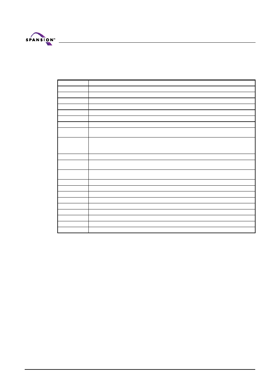
Table 3.1 identifies the input and output package connections provided on the device.
Table 3.1 Input/Output Descriptions
Symbol
Description
A23-A0
Address inputs
DQ15-DQ0
Data input/output
OE#
Output Enable input. Asynchronous relative to CLK for the Burst mode.
WE#
Write Enable input.
VSS
Ground
NC
No Connect; not connected internally
RDY
Ready output. Indicates the status of the Burst read. The WAIT# pin of the pSRAM is tied to RDY.
CLK
Clock input. In burst mode, after the initial word is output, subsequent active edges of CLK increment the internal
address counter. Should be at VIL or VIH while in asynchronous mode
AVD#
Address Valid input. Indicates to device that the valid address is present on the address inputs.
Low = for asynchronous mode, indicates valid address; for burst mode, causes starting address to be latched.
High = device ignores address inputs
F-RST#
Hardware reset input. Low = device resets and returns to reading array data
F-WP#
Hardware write protect input. At VIL, disables program and erase functions in the four outermost sectors. Should be
at VIH for all other conditions.
F-ACC
Accelerated input. At VHH, accelerates programming; automatically places device in unlock bypass mode. At VIL,
disables all program and erase functions. Should be at VIH for all other conditions.
R-CE1#
Chip-enable input for pSRAM.
F1-CE#
Chip-enable input for Flash 1. Asynchronous relative to CLK for Burst Mode.
F2-CE#
Chip-enable input for Flash 2. Asynchronous relative to CLK for Burst Mode. This applies to the 512Mb MCP only.
R-CRE
Control Register Enable (pSRAM). For CellularRAM only.
F-VCC
Flash 1.8 Volt-only single power supply.
R-VCC
pSRAM Power Supply.
R-UB#
Upper Byte Control (pSRAM).
R-LB#
Lower Byte Control (pSRAM)
DNU
Do Not Use
相關(guān)PDF資料 |
PDF描述 |
|---|---|
| S7DB-04C500R | 1-OUTPUT 20 W DC-DC REG PWR SUPPLY MODULE |
| S894-10-068-00-240000 | PLCC68, IC SOCKET |
| S894-90-068-00-241100 | PLCC68, IC SOCKET |
| S894-90-068-00-240100 | PLCC68, IC SOCKET |
| S894-90-068-00-240000 | PLCC68, IC SOCKET |
相關(guān)代理商/技術(shù)參數(shù) |
參數(shù)描述 |
|---|---|
| S71WS512NC0BAWTK2 | 制造商:SPANSION 制造商全稱:SPANSION 功能描述:Stacked Multi-Chip Product (MCP) |
| S71WS512NC0BAWTK3 | 制造商:SPANSION 制造商全稱:SPANSION 功能描述:Stacked Multi-Chip Product (MCP) |
| S71WS512NC0BAWTN0 | 制造商:SPANSION 制造商全稱:SPANSION 功能描述:Stacked Multi-Chip Product (MCP) |
| S71WS512NC0BAWTN2 | 制造商:SPANSION 制造商全稱:SPANSION 功能描述:Stacked Multi-Chip Product (MCP) |
| S71WS512NC0BAWTN3 | 制造商:SPANSION 制造商全稱:SPANSION 功能描述:Stacked Multi-Chip Product (MCP) |
發(fā)布緊急采購,3分鐘左右您將得到回復(fù)。