- 您現(xiàn)在的位置:買賣IC網(wǎng) > PDF目錄373355 > S80016LK7MK8TW-8A (Electronic Theatre Controls, Inc.) SYVCHRONOUS DRAM PDF資料下載
參數(shù)資料
| 型號(hào): | S80016LK7MK8TW-8A |
| 廠商: | Electronic Theatre Controls, Inc. |
| 英文描述: | SYVCHRONOUS DRAM |
| 中文描述: | SYVCHRONOUS內(nèi)存 |
| 文件頁數(shù): | 4/9頁 |
| 文件大小: | 361K |
| 代理商: | S80016LK7MK8TW-8A |
128Mb: x4, x8, x16
SDRAM 3.3V
PDF: 09005aef807827f6 / Source: 09005aef807825bd
128Mb SDRAM
Rev: 11/29/2004
4
SpecTek reserves the right to change products or specifications without notice.
2001, 2002, 2004 SpecTek
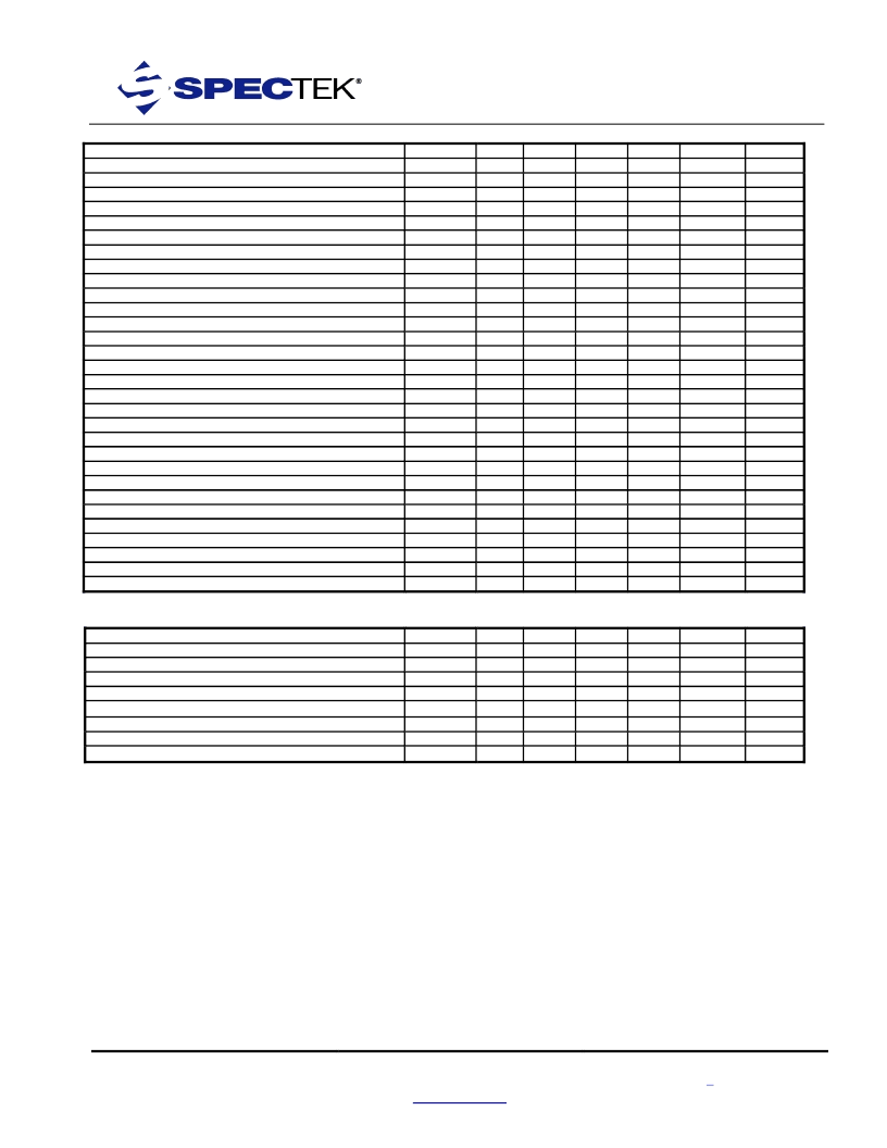
AC ELECTRICAL CHARACTERISTICS:
Vdd = 3.3V
±
10%V, Temp. = 25
°
to 70
°
C
AC CHARACTERISTICS
PARAMETER
Access time from CLK (positive edge) CL = 3
Access time from CLK (positive edge) CL = 2
Address hold time
Address setup time
CLK high level width
CLK low level width
Clock cycle time CL = 3
Clock cycle time CL = 2
CKE hold time
CKE setup time
CS#, RAS#, CAS#, WE#, DQM hold time
CS#, RAS#, CAS#, WE#, DQM setup time
Data-in hold time
Data-in setup time
Data-out high impedance time
Data-out low impedance time
Data-out hold time
ACTIVE to PRECHARGE command period
AUTO REFRESH to ACTIVE command period
ACTIVE to READ or WRITE delay
Refresh period (4096 cycles)
PRECHARGE command period
ACTIVE bank A to bank B command period
Transition time
Write recovery time
Exit SELF REFRESH to ACTIVE command
READ/WRITE command to READ/WRITE command
CKE to clock disable or power down entry mode
CKE to clock enable or power down exit setup
-75A
MIN
-75A
MAX
5.4
N/A
-8A
MIN
-8A
MAX
6
SYMBOL
tAC
tAC
tAH
tAS
tCH
tCL
tCK
tCK
tCKH
tCKS
tCMH
tCMS
tDH
tDS
tHZ
tLZ
tOH
tRAS
tRC
tRCD
tREF
tRP
tRRD
tT
tWR
tXSR
tCCD
tCKED
tPED
UNITS
ns
ns
ns
ns
ns
ns
ns
ns
ns
ns
ns
ns
ns
ns
ns
ns
ns
ns
ns
ns
ms
ns
ns
ns
ns
tCK
tCK
tCK
tCK
NOTES
0.8
1.5
2.5
2.5
7.5
N/A
0.8
1.5
0.8
1.5
0.8
1.5
1
2
3
3
10
1
2
1
2
1
2
9
9
4
1
2
3
2.7
44
60
22.5
16K
50
80
30
16K
64
64
22.5
15
0.3
20
8
1
1
1
30
20
0.3
20
8
1
1
1
2
2
3
1
2
2
AC ELECTRICAL CHARACTERISTICS:
Vdd = 3.3V
±
10%V, Temp. = 25
°
to 70
°
C
AC CHARACTERISTICS
PARAMETER
DQM to input data delay
WRITE command to input data delay
Data-in to ACTIVATE command w/ Auto precharge
Data-in to precharge
Last data-in to precharge command
LOAD MODE REGISTER command to command
Data-out to high impedance from precharge
-75A
MIN
0
0
5
2
2
2
3
-75A
MAX
-8
-8
SYMBOL
tDQD
tDWD
tDAL
tDPL
tRDL
tMRD
tROH
MIN
0
0
5
2
2
2
3
MAX
UNITS
tCK
tCK
tCK
tCK
tCK
tCK
tCK
NOTES
1
1
3
2, 3
1
1
1
NOTES:
1.
2.
3.
4.
Clocks required specified by JEDEC functionality and not dependent on any timing parameter.
Timing actually specified by tCKS, clock(s) specified as a reference only at a minimum cycle rate.
Timing actually specified by tWR plus tRP clock(s) specified as a reference only at a minimum cycle rate.
tHZ defines the time at which the output achieves the open circuit condition; it is not a reference to Voh or Vol. The last valid data
element will meet tOH before going high-Z.
Based on tCK = 10ns for –8 and tCK = 7.5ns for –75a
5.
相關(guān)PDF資料 |
PDF描述 |
|---|---|
| S80016LK7MK9TW-75A | SYVCHRONOUS DRAM |
| S80016LK7MK9TW-8A | SYVCHRONOUS DRAM |
| S8046 | Photo IC for optical link |
| S8119 | MOSFET, Switching; VDSS (V): 60; ID (A): 1.5; Pch : 0.8; RDS (ON) typ. (ohm) @10V: -; RDS (ON) typ. (ohm) @4V[4.5V]: [0.173]; RDS (ON) typ. (ohm) @2.5V: 0.207; Ciss (pF) typ: 200; toff (µs) typ: 0.035; Package: MPAK |
| S8193 | Si photodiode Detector for X-ray monitors |
相關(guān)代理商/技術(shù)參數(shù) |
參數(shù)描述 |
|---|---|
| S80016LK7MK9FB-75A | 制造商:未知廠家 制造商全稱:未知廠家 功能描述:SYVCHRONOUS DRAM |
| S80016LK7MK9FB-8A | 制造商:未知廠家 制造商全稱:未知廠家 功能描述:SYVCHRONOUS DRAM |
| S80016LK7MK9FC-75A | 制造商:未知廠家 制造商全稱:未知廠家 功能描述:SYVCHRONOUS DRAM |
| S80016LK7MK9FC-8A | 制造商:未知廠家 制造商全稱:未知廠家 功能描述:SYVCHRONOUS DRAM |
| S80016LK7MK9TW-75A | 制造商:未知廠家 制造商全稱:未知廠家 功能描述:SYVCHRONOUS DRAM |
發(fā)布緊急采購,3分鐘左右您將得到回復(fù)。