- 您現(xiàn)在的位置:買賣IC網(wǎng) > PDF目錄372096 > S83C752-1A28 (NXP SEMICONDUCTORS) 80C51 8-bit microcontroller family 2K/64 OTP/ROM, 5 channel 8 bit A/D, I2C, PWM, low pin count PDF資料下載
參數(shù)資料
| 型號(hào): | S83C752-1A28 |
| 廠商: | NXP SEMICONDUCTORS |
| 元件分類: | 微控制器/微處理器 |
| 英文描述: | 80C51 8-bit microcontroller family 2K/64 OTP/ROM, 5 channel 8 bit A/D, I2C, PWM, low pin count |
| 中文描述: | 8-BIT, MROM, 12 MHz, MICROCONTROLLER, PQCC28 |
| 文件頁數(shù): | 11/24頁 |
| 文件大小: | 225K |
| 代理商: | S83C752-1A28 |

Philips Semiconductors
Product specification
83C752/87C752
80C51 8-bit microcontroller family
2K/64 OTP/ROM, 5 channel 8 bit A/D, I
2
C, PWM, low pin count
1998 May 01
11
R
S
V
ANALOG
INPUT
C
S
C
C
To Comparator
+
I
N
I
N+1
Sm
N+1
Sm
N
Rm
N+1
Rm
N
Multiplexer
Rm = 0.5 - 3 k
CS + CC = 15pF maximum
RS = Recommended < 9.6 k
for 1 LSB @ 12MHz
NOTE:
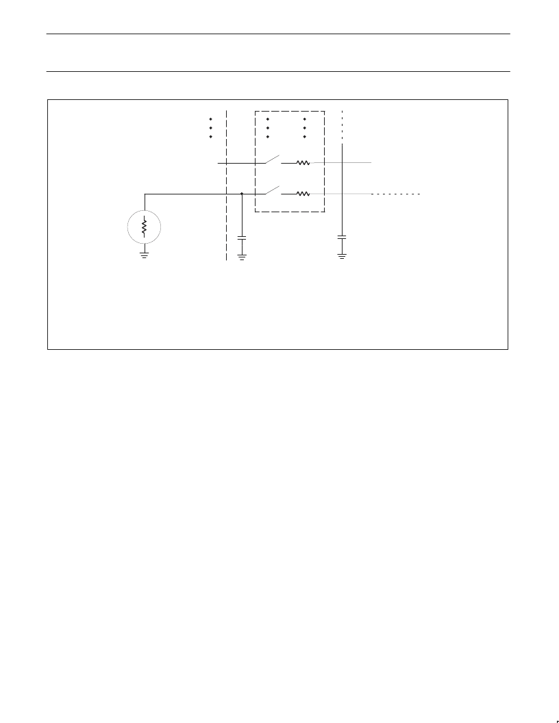
Because the analog to digital converter has a sampled-data comparator, the input looks capacitive to a source. When a conversion
is initiated, switch Sm closes for 8tcy (8
μ
s @ 12MHz crystal frequency) during which time capacitance Cs + Cc is charged. It should
be noted that the sampling causes the analog input to present a varying load to an analog source.
SU00199
Figure 2. A/D Input: Equivalent Circuit
A/D CONVERTER PARAMETER DEFINITIONS
The following definitions are included to clarify some specifications
given and do not represent a complete set of A/D parameter
definitions.
Absolute Accuracy Error
Absolute accuracy error of a given output is the difference between
the theoretical analog input voltage to produce a given output and
the actual analog input voltage required to produce the same code.
Since the same output code is produced by a band of input voltages,
the “required input voltage” is defined as the midpoint of the band of
input voltage that will produce that code. Absolute accuracy error
not specified with a code is the maximum over all codes.
Nonlinearity
If a straight line is drawn between the end points of the actual
converter characteristics such that zero offset and full scale errors
are removed, then non-linearity is the maximum deviation of the
code transitions of the actual characteristics from that of the straight
line so constructed. This is also referred to as relative accuracy and
also integral non-linearity.
Differential Non-Linearity
Differential non-linearity is the maximum difference between the
actual and ideal code widths of the converter. The code widths are
the differences expressed in LSB between the code transition
points, as the input voltage is varied through the range for the
complete set of codes.
Gain Error
Gain error is the deviation between the ideal and actual analog input
voltage required to cause the final code transition to a full-scale
output code after the offset error has been removed. This may
sometimes be referred to as full scale error.
Offset Error
Offset error is the difference between the actual input voltage that
causes the first code transition and the ideal value to cause the first
code transition. This ideal value is 1/2 LSB above V
ref–
.
Channel to Channel Matching
Channel to channel matching is the maximum difference between
the corresponding code transitions of the actual characteristics
taken from different channels under the same temperature, voltage
and frequency conditions.
Crosstalk
Crosstalk is the measured level of a signal at the output of the
converter resulting from a signal applied to one deselected channel.
Total Error
Maximum deviation of any step point from a line connecting the ideal
first transition point to the ideal last transition point.
Relative Accuracy
Relative accuracy error is the deviation of the ADC’s actual code
transition points from the ideal code transition points on a straight
line which connects the ideal first code transition point and the final
code transition point, after nullifying offset error and gain error. It is
generally expressed in LSBs or in percent of FSR.
相關(guān)PDF資料 |
PDF描述 |
|---|---|
| S83C752-1DB | 80C51 8-bit microcontroller family 2K/64 OTP/ROM, 5 channel 8 bit A/D, I2C, PWM, low pin count |
| S83C752-1N28 | 80C51 8-bit microcontroller family 2K/64 OTP/ROM, 5 channel 8 bit A/D, I2C, PWM, low pin count |
| S83C752-2N28 | 80C51 8-bit microcontroller family 2K/64 OTP/ROM, 5 channel 8 bit A/D, I2C, PWM, low pin count |
| S83C752-4A28 | 80C51 8-bit microcontroller family 2K/64 OTP/ROM, 5 channel 8 bit A/D, I2C, PWM, low pin count |
| S83C752-4DB | 80C51 8-bit microcontroller family 2K/64 OTP/ROM, 5 channel 8 bit A/D, I2C, PWM, low pin count |
相關(guān)代理商/技術(shù)參數(shù) |
參數(shù)描述 |
|---|---|
| S83C752-1DB | 制造商:PHILIPS 制造商全稱:NXP Semiconductors 功能描述:80C51 8-bit microcontroller family 2K/64 OTP/ROM, 5 channel 8 bit A/D, I2C, PWM, low pin count |
| S83C752-1N28 | 制造商:PHILIPS 制造商全稱:NXP Semiconductors 功能描述:80C51 8-bit microcontroller family 2K/64 OTP/ROM, 5 channel 8 bit A/D, I2C, PWM, low pin count |
| S83C752-2A28 | 制造商:PHILIPS 制造商全稱:NXP Semiconductors 功能描述:80C51 8-bit microcontroller family 2K/64 OTP/ROM, 5 channel 8 bit A/D, I2C, PWM, low pin count |
| S83C752-2N28 | 制造商:PHILIPS 制造商全稱:NXP Semiconductors 功能描述:80C51 8-bit microcontroller family 2K/64 OTP/ROM, 5 channel 8 bit A/D, I2C, PWM, low pin count |
| S83C752-4A28 | 制造商:PHILIPS 制造商全稱:NXP Semiconductors 功能描述:80C51 8-bit microcontroller family 2K/64 OTP/ROM, 5 channel 8 bit A/D, I2C, PWM, low pin count |
發(fā)布緊急采購,3分鐘左右您將得到回復(fù)。