- 您現(xiàn)在的位置:買賣IC網(wǎng) > PDF目錄192306 > S9705 LOGIC OUTPUT PHOTO DETECTOR PDF資料下載
參數(shù)資料
| 型號: | S9705 |
| 元件分類: | 光電元器件 |
| 英文描述: | LOGIC OUTPUT PHOTO DETECTOR |
| 封裝: | PLASTIC PACKAGE-4 |
| 文件頁數(shù): | 2/2頁 |
| 文件大?。?/td> | 0K |
| 代理商: | S9705 |
Light-to-frequency converter photo IC
S9705
HAMAMATSU PHOTONICS K.K., Solid State Division
1126-1 Ichino-cho, Higashi-ku, Hamamatsu City, 435-8558 Japan, Telephone: (81) 53-434-3311, Fax: (81) 53-434-5184, www.hamamatsu.com
U.S.A.: Hamamatsu Corporation: 360 Foothill Road, P.O.Box 6910, Bridgewater, N.J. 08807-0910, U.S.A., Telephone: (1) 908-231-0960, Fax: (1) 908-231-1218
Germany: Hamamatsu Photonics Deutschland GmbH: Arzbergerstr. 10, D-82211 Herrsching am Ammersee, Germany, Telephone: (49) 08152-3750, Fax: (49) 08152-2658
France: Hamamatsu Photonics France S.A.R.L.: 19, Rue du Saule Trapu, Parc du Moulin de Massy, 91882 Massy Cedex, France, Telephone: 33-(1) 69 53 71 00, Fax: 33-(1) 69 53 71 10
United Kingdom: Hamamatsu Photonics UK Limited: 2 Howard Court, 10 Tewin Road, Welwyn Garden City, Hertfordshire AL7 1BW, United Kingdom, Telephone: (44) 1707-294888, Fax: (44) 1707-325777
North Europe: Hamamatsu Photonics Norden AB: Smidesvgen 12, SE-171 41 Solna, Sweden, Telephone: (46) 8-509-031-00, Fax: (46) 8-509-031-01
Italy: Hamamatsu Photonics Italia S.R.L.: Strada della Moia, 1/E, 20020 Arese, (Milano), Italy, Telephone: (39) 02-935-81-733, Fax: (39) 02-935-81-741
Information furnished by HAMAMATSU is believed to be reliable. However, no responsibility is assumed for possible inaccuracies or omissions.
Specifications are subject to change without notice. No patent rights are granted to any of the circuits described herein. 2007 Hamamatsu Photonics K.K.
Cat. No. KPIC1059E06
Oct. 2007 DN
2
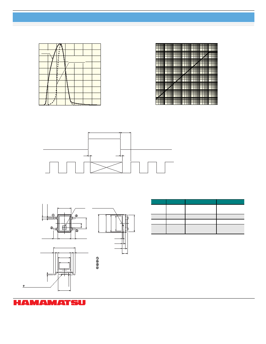
s Spectral response
KPICA0063EC
WAVELENGTH (nm)
RELATIVE
SENSITIVITY
600
500
400
900
800
700
1000
(Typ. Ta=25 C)
300
0
0.2
0.4
0.6
0.8
1.0
S9705
HUMAN EYE
SENSITIVITY
s Output frequency vs. illuminance
ILLUMINANCE (lx)
OUTPUT
FREQUENCY
(Hz)
(Typ. Ta=25 C, 2856 K)
10
-3
10
-2
10
-1
10
0
10
1
10
2
10
3
10
-1
10
0
10
1
10
2
10
3
10
4
10
5
10
6
10
7
10
4
OUTPUT
RESET *2
td
Note)
*2: OUTPUT terminal is at High impedance during RESET period ("High" state).
*3: Output starts with "Low" after releasing RESET. Illuminance can be obtained by measuring the time (tor) required
before the first output transition after releasing RESET. (tres is recommended to be longer than 1 s.)
tres
tor *3
s Timing chart
s Dimensional outline (unit: mm)
KPICC0120ED
3.4
3.8
4.0
*
4.2
±
0.2
(INCLUDING
BURR)
3.9
0.05
0.75
1.3
RESET
GND
Vdd
OUTPUT
Tolerance unless otherwise
noted: ±0.1, ±2
Shaded area indicates burr.
Chip position accuracy with
respect to the package
dimensions marked *
X, Y
≤±0.2, θ≤±3
PHOTOSENSITIVE
SURFACE
2.4
MIRROR AREA
RANGE
2.8
3.0 *
0.45 ± 0.3
5.0 ± 0.3
0.15
0.1
±
0.1
2.9
1.8 DEPTH 0.15 MAX.
(E.PIN)
3.2 ± 0.2
(INCLUDING BURR)
ACTIVE
AREA
(4
×
)0.35
(4
×
)0.45
2.54
3.0 *
1.0 ± 0.4
0.35
0.75
KPICB0093EB
KPICB0091EC
s Pin connection
Pin No.
Symbol
Function
Input/Output
1
RESET
Out disable
Input
(digital)
2
GND
Ground
-
3
Vdd
Supply terminal
-
4
OUTPUT Output terminal
Output
(digital)
相關(guān)PDF資料 |
PDF描述 |
|---|---|
| SA020-403T | SIP20, IC SOCKET |
| SA030-398G | SIP30, IC SOCKET |
| SA05-11SRWA | 7 SEG NUMERIC DISPLAY, SUPER BRIGHT RED, 12.7 mm |
| SA08-12SURKWA | 7 SEG NUMERIC DISPLAY, HYPER RED, 20.32 mm |
| SA0805175NSTER | ACTIVE DELAY LINE, TRUE OUTPUT, CSIP8 |
相關(guān)代理商/技術(shù)參數(shù) |
參數(shù)描述 |
|---|---|
| S9706 | 制造商:Hamamatsu Photonics 功能描述: |
| S971 | 制造商:EPCOS 制造商全稱:EPCOS 功能描述:NTC thermistors for temperature measurement |
| S9717 | 制造商:HAMAMATSU 制造商全稱:Hamamatsu Corporation 功能描述:Si APD High reliability, surface-mount ceramic package |
| S9717_11 | 制造商:HAMAMATSU 制造商全稱:Hamamatsu Corporation 功能描述:High reliability, surface-mount ceramic package |
| S9717-02K | 制造商:HAMAMATSU 制造商全稱:Hamamatsu Corporation 功能描述:Si APD High reliability, surface-mount ceramic package |
發(fā)布緊急采購,3分鐘左右您將得到回復(fù)。