- 您現(xiàn)在的位置:買賣IC網(wǎng) > PDF目錄385813 > SAA7111 (NXP Semiconductors N.V.) Video Input Processor VIP PDF資料下載
參數(shù)資料
| 型號: | SAA7111 |
| 廠商: | NXP Semiconductors N.V. |
| 英文描述: | Video Input Processor VIP |
| 中文描述: | 視頻輸入處理器貴賓 |
| 文件頁數(shù): | 7/64頁 |
| 文件大小: | 433K |
| 代理商: | SAA7111 |
第1頁第2頁第3頁第4頁第5頁第6頁當(dāng)前第7頁第8頁第9頁第10頁第11頁第12頁第13頁第14頁第15頁第16頁第17頁第18頁第19頁第20頁第21頁第22頁第23頁第24頁第25頁第26頁第27頁第28頁第29頁第30頁第31頁第32頁第33頁第34頁第35頁第36頁第37頁第38頁第39頁第40頁第41頁第42頁第43頁第44頁第45頁第46頁第47頁第48頁第49頁第50頁第51頁第52頁第53頁第54頁第55頁第56頁第57頁第58頁第59頁第60頁第61頁第62頁第63頁第64頁
1998 May 15
7
Philips Semiconductors
Product specification
Video Input Processor (VIP)
SAA7111
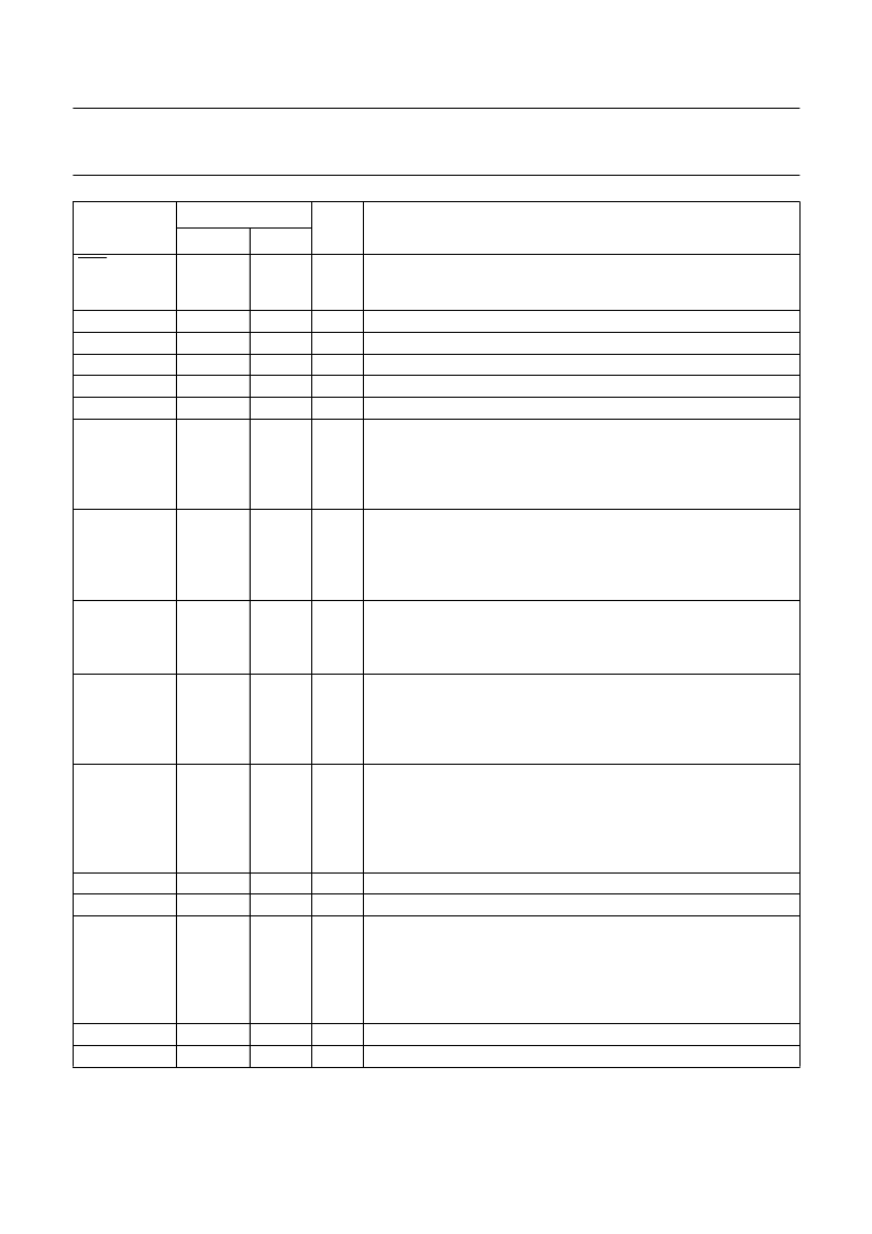
RES
32
23
O
Reset output (active LOW); sets the device into a defined state.
All data outputs are in high impedance state. The I
2
C-bus is reset
(waiting for start condition) note 4.
Chip enable; connection to ground forces a reset.
Positive digital supply voltage 4 (+5 V).
Digital ground for positive supply voltage 4.
Not connected.
Not connected.
Horizontal sync output signal (programmable); the positions of the
positive and negative slopes are programmable in 8 LLC increments
over a complete line (equals 64
μ
s) via I
2
C-bus bytes HSB and HSS.
Fine position adjustment in 2 LLC increments can be performed via
I
2
C-bits HDEL1 and HDEL0.
Two functions output; controlled by I
2
C-bit RTSE1.
RTSE1 = 0: PAL line identifier (LOW = PAL line); indicates the
inverted and non-inverted R
Y component for PAL signals.
RTSE1 = 1: H-PLL locked indicator; a high state indicates that the
internal horizontal PLL has locked.
Two functions output; controlled by I
2
C-bit RTSE0.
RTSE0 = 0: odd/even field identification (HIGH = odd field).
RTSE0 = 1: vertical locked indicator; a HIGH state indicates that the
internal VNL has locked.
Vertical sync output signal (enabled via I
2
C-bit OEHV); this signal
indicates the vertical sync with respect to the YUV output. The HIGH
period of this signal is approximately six lines if the vertical noise
limiter (VNL) function is active. The positive slope contains the phase
information for a deflection controller.
Horizontal reference output signal (enabled via I
2
C-bit OEHV); this
signal is used to indicate data on the digital YUV bus. The positive
slope marks the beginning of a new active line. The HIGH period of
HREF is 720 Y samples long. HREF can be used to synchronize data
multiplexer/demultiplexers. HREF is also present during the vertical
blanking interval.
Digital ground for positive supply voltage 3.
Positive digital supply voltage 3 (+5 V).
Digital VPO-bus (Video Port Out) output signal; higher bits of the
16-bit YUV-bus or the 16-bit RGB-bus output signal. The output data
rate, the format and multiplexing scheme of the VPO-bus are
controlled via I
2
C-bits OFTS0 and OFTS1. With I
2
C-bit VIPB = 1 the
six MSBs of the digitized input signal (AD1 [7 to 2]) are connected to
these outputs.
Digital ground for positive supply voltage 2.
Positive digital supply voltage 2 (+5 V).
CE
V
DD4
V
SS4
n.c.
n.c.
HS
33
34
35
36
37
38
24
25
26
27
I
P
GND
O
RTS1
39
28
O
RTS0
40
29
O
VS
41
30
O
HREF
42
31
O
V
SS3
V
DD3
VPO (15 to 10)
43
44
32
33
GND
P
O
45 to 50
34 to 39
V
SS2
V
DD2
51
52
40
41
GND
P
SYMBOL
PINS
I/O
DESCRIPTION
PLCC68
QFP64
相關(guān)PDF資料 |
PDF描述 |
|---|---|
| SAA7120H | Digital video encoder |
| SAA7152 | Digital Video Comb Filter DCF |
| SAA7184 | Digital Video Encoders DENC2-M6 |
| SAA7187 | Digital video encoder (DENC2-SQ)(數(shù)字視頻編碼器) |
| SAA7188A | Digital Video Encoder (DENC2-M)(數(shù)字視頻編碼器(DENC2-M)) |
相關(guān)代理商/技術(shù)參數(shù) |
參數(shù)描述 |
|---|---|
| SAA7111A | 制造商:PHILIPS 制造商全稱:NXP Semiconductors 功能描述:Enhanced Video Input Processor EVIP |
| SAA7111AH | 制造商:NXP Semiconductors 功能描述: 制造商:Philips Semiconductor 功能描述: 制造商:NXP Semiconductors 功能描述:TV/VIDEO SIGNAL PROCESSOR, 64 Pin, Plastic, QFP |
| SAA7111AH/V4,557 | 功能描述:視頻 IC ENHANCED VIDEO INPUT RoHS:否 制造商:Fairchild Semiconductor 工作電源電壓:5 V 電源電流:80 mA 最大工作溫度:+ 85 C 封裝 / 箱體:TSSOP-28 封裝:Reel |
| SAA7111AHBG | 功能描述:視頻 IC ENHANCED VIDEO INPUT PROCESSOR RoHS:否 制造商:Fairchild Semiconductor 工作電源電壓:5 V 電源電流:80 mA 最大工作溫度:+ 85 C 封裝 / 箱體:TSSOP-28 封裝:Reel |
| SAA7111AHZ | 制造商:NXP Semiconductors 功能描述: |
發(fā)布緊急采購,3分鐘左右您將得到回復(fù)。