- 您現(xiàn)在的位置:買賣IC網(wǎng) > PDF目錄271679 > SD-14551DX-304K (DATA DEVICE CORP) SYNCHRO OR RESOLVER TO DIGITAL CONVERTER, CQIP34 PDF資料下載
參數(shù)資料
| 型號(hào): | SD-14551DX-304K |
| 廠商: | DATA DEVICE CORP |
| 元件分類: | 位置變換器 |
| 英文描述: | SYNCHRO OR RESOLVER TO DIGITAL CONVERTER, CQIP34 |
| 封裝: | CERAMIC, DIP-34 |
| 文件頁(yè)數(shù): | 7/12頁(yè) |
| 文件大?。?/td> | 115K |
| 代理商: | SD-14551DX-304K |

4
Data Device Corporation
www.ddc-web.com
SD-14550 Series
Rev. H
GENERAL SETUP CONSIDERATIONS
The following recommendations should be considered when
using the SD-14550 Series converters:
1) The power supply is +5 V DC.
2) Direct inputs are referenced to AGND.
3) Connect (close to hybrid) pin 31 (Analog Ground) to pin 7
(GND).
4) Connect a 33 F/10 VDC tantalum filter capacitor externally
between pin 5 (filter point) to pin 7 (ground).
PROGRAMMABLE RESOLUTION
Resolution is controlled by pins 27 and 28. The resolution can be
changed during converter operation so that the appropriate res-
olution and velocity dynamics can be set as needed. To insure
that a race condition does not exist between counting and
changing the resolution, the resolution control is latched inter-
nally. Refer to TABLE 2 for resolution control.
BIT (BUILT-IN-TEST)
This output is a logic line that will flag an internal fault condition
or LOS (Loss-Of-Signal). The internal fault detector monitors the
internal loop error and, when it exceeds approximately ±100
LSBs, will set the line to a logic 0; this condition will occur during
a large-step input and will reset to a logic 1 after the converter
settles out. (The error voltage is filtered with a 500 s filter.) BIT
will set for an over velocity condition because the converter loop
cannot maintain input/output sync. BIT will also be set if a total
LOS (loss of all signals) occurs. Additionally, in the SD-14550XS
version, BIT will set when a Loss-of-Reference (LOR) condition
occurs.
THEORY OF OPERATION
The SD-14550 Series of converters are based upon a single
chip CMOS custom monolithic. They are implemented using the
latest IC technology, which merges precision analog circuitry
with digital logic to form a complete high performance tracking
synchro/resolver-to-digital converter.
CONVERTER OPERATION
FIGURE 1 is the functional block diagram of the SD-14550
Series. The converter operates with a single +5 V DC power sup-
ply and internally generates a negative voltage of approximate-
ly 5 volts. This negative voltage comes out on pin 5 (filter point)
— see GENERAL SETUP CONSIDERATIONS.
The converter is made up of three main sections; an input front-
end, an error processor, and a digital interface. The converter
front-end differs for synchro, resolver and direct inputs. An elec-
tronic Scott-T is used for synchro inputs, a resolver conditioner
for resolver inputs, and a sine and cosine voltage follower for
direct inputs. These amplifiers feed the high accuracy Control
Transformer (CT). Its other input is the 16-bit digital angle
φ. Its
output is an analog error angle, or difference angle, between the
two inputs. The CT performs the ratiometric trigonometric com-
putation of SIN
θCOSφ - COSθSINφ = SIN(θ - φ) using amplifiers,
switches, logic, and capacitors in precision ratios.
The converter accuracy is limited by the precision of the com-
puting elements in the CT. In these converters ratioed capacitors
are used in the CT, instead of the more conventional precision
ratioed resistors. Capacitors used as computing elements with
op-amps need to be sampled to eliminate voltage drifting.
Therefore, the circuits are sampled at a high rate to eliminate
this drifting and at the same time to cancel out the op-amp off-
sets.
The error processing is performed using the industry standard
technique for type II tracking R/D converters. The DC error is
integrated yielding a velocity voltage which in turn drives a volt-
age controlled oscillator (VCO). This VCO is an incremental inte-
grator (constant voltage input to position rate output) which
together with the velocity integrator forms a type II servo feed-
back loop. A lead in the frequency response is introduced to sta-
bilize the loop and another lag at higher frequency is introduced
to reduce the gain and ripple at the carrier frequency and above.
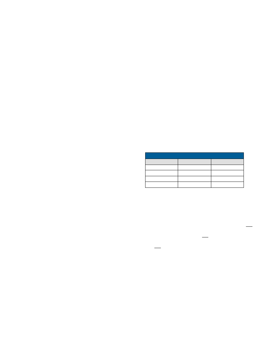
TABLE 2. RESOLUTION CONTROL (A AND B)
RESOLUTION
B
A
10 bit
0
12 bit
0
1
14 bit
1
0
16 bit
1
相關(guān)PDF資料 |
PDF描述 |
|---|---|
| SD-14554DX-332Z | SYNCHRO OR RESOLVER TO DIGITAL CONVERTER, CQIP34 |
| SD-14620DX-184W | SYNCHRO OR RESOLVER TO DIGITAL CONVERTER, CQIP54 |
| SD-14620DX-194L | SYNCHRO OR RESOLVER TO DIGITAL CONVERTER, CQIP54 |
| SD-14623DX-242L | SYNCHRO OR RESOLVER TO DIGITAL CONVERTER, CQIP54 |
| SD-14623DX-272W | SYNCHRO OR RESOLVER TO DIGITAL CONVERTER, CQIP54 |
相關(guān)代理商/技術(shù)參數(shù) |
參數(shù)描述 |
|---|---|
| SD1456 | 功能描述:射頻雙極電源晶體管 NPN 28V 170-230MHz RoHS:否 制造商:M/A-COM Technology Solutions 配置:Single 直流集電極/Base Gain hfe Min:40 最大工作頻率:30 MHz 集電極—發(fā)射極最大電壓 VCEO:25 V 發(fā)射極 - 基極電壓 VEBO:4 V 集電極連續(xù)電流:20 A 最大直流電集電極電流: 功率耗散:250 W 封裝 / 箱體:Case 211-11 封裝:Tray |
| SD1457 | 功能描述:射頻放大器 RF Bipolar Trans RoHS:否 制造商:Skyworks Solutions, Inc. 類型:Low Noise Amplifier 工作頻率:2.3 GHz to 2.8 GHz P1dB:18.5 dBm 輸出截獲點(diǎn):37.5 dBm 功率增益類型:32 dB 噪聲系數(shù):0.85 dB 工作電源電壓:5 V 電源電流:125 mA 測(cè)試頻率:2.6 GHz 最大工作溫度:+ 85 C 安裝風(fēng)格:SMD/SMT 封裝 / 箱體:QFN-16 封裝:Reel |
| SD1458 | 功能描述:射頻放大器 RF Bipolar Trans RoHS:否 制造商:Skyworks Solutions, Inc. 類型:Low Noise Amplifier 工作頻率:2.3 GHz to 2.8 GHz P1dB:18.5 dBm 輸出截獲點(diǎn):37.5 dBm 功率增益類型:32 dB 噪聲系數(shù):0.85 dB 工作電源電壓:5 V 電源電流:125 mA 測(cè)試頻率:2.6 GHz 最大工作溫度:+ 85 C 安裝風(fēng)格:SMD/SMT 封裝 / 箱體:QFN-16 封裝:Reel |
| SD1459 | 功能描述:射頻雙極電源晶體管 NPN 28V 170-230MHz RoHS:否 制造商:M/A-COM Technology Solutions 配置:Single 直流集電極/Base Gain hfe Min:40 最大工作頻率:30 MHz 集電極—發(fā)射極最大電壓 VCEO:25 V 發(fā)射極 - 基極電壓 VEBO:4 V 集電極連續(xù)電流:20 A 最大直流電集電極電流: 功率耗散:250 W 封裝 / 箱體:Case 211-11 封裝:Tray |
| SD-14595D1-102 | 制造商:未知廠家 制造商全稱:未知廠家 功能描述:Synchro-to-Digital Converter |
發(fā)布緊急采購(gòu),3分鐘左右您將得到回復(fù)。