- 您現(xiàn)在的位置:買(mǎi)賣(mài)IC網(wǎng) > PDF目錄271661 > SD-14591D1-364L (DATA DEVICE CORP) SYNCHRO OR RESOLVER TO DIGITAL CONVERTER, MDIP36 PDF資料下載
參數(shù)資料
| 型號(hào): | SD-14591D1-364L |
| 廠商: | DATA DEVICE CORP |
| 元件分類: | 位置變換器 |
| 英文描述: | SYNCHRO OR RESOLVER TO DIGITAL CONVERTER, MDIP36 |
| 封裝: | DDIP-36 |
| 文件頁(yè)數(shù): | 11/16頁(yè) |
| 文件大小: | 152K |
| 代理商: | SD-14591D1-364L |
第1頁(yè)第2頁(yè)第3頁(yè)第4頁(yè)第5頁(yè)第6頁(yè)第7頁(yè)第8頁(yè)第9頁(yè)第10頁(yè)當(dāng)前第11頁(yè)第12頁(yè)第13頁(yè)第14頁(yè)第15頁(yè)第16頁(yè)

4
Data Device Corporation
www.ddc-web.com
SD-14590/91/92
D-02/02-250
TABLE 1. SD-14590/91/92 SPECIFICATIONS (CONT.)
These specifications apply over the rated power supply, temperature,
and reference frequency ranges; 10% signal amplitude variation and
10% harmonic distortion.
VALUE
PARAMETER
TRANSFORMER
CHARACTERISTICS (CONT’D)
Signal Transformer
Carrier Frequency Range
Breakdown Voltage to GND
Minimum Input Impedances
(Balanced)
90V L-L
26V L-L
11.8V L-L
60 Hz TRANSFORMERS
Reference Transformer
Carrier Frequency Range
Input Voltage Range
Input Impedance
Input Common Mode Voltage
Output Description
Output Voltage
Power Required
Signal Transformer
Carrier Frequency Range
Input Voltage Range
Input Impedance
Input Common Mode Voltage
Output Description
Output Voltage
Power Required
360 - 1000 Hz
700 V peak
Synchro ZIN(ZSO) Resolver ZIN
180
100k
—
30k
20k
30k
47 - 440 Hz
80 - 138 V rms; 115 V rms
nominal resistive
600 K
min resistive
500 V rms transformer isolated
+R (in phase with RH-RL) and -R (in
phase with RL-RH) derived from op-
amps. Short-Circuit proof.
3.0 V nominal riding on ground refer-
ence V. Output Voltage level tracks
input level.
4 mA typ, 7 mA max from +15 V
supply.
47 - 440 Hz
10 - 100 V rms L-L; 90 V rms L-L
nominal
148 k
min L-L balanced resistive
±500 V rms transformer isolated
Resolver Output:
- sine (-S) + cosine (+C) derived
from op-amps.
Short-circuit proof.
1.0 V rms nominal riding on ground
reference V. Output Voltage level
tracks input level.
4 mA typ, 7 mA max from +15 V
supply.
NOTES:
1. Pin programmable for SD-14590 only; SD-14591 is 14 bits and
SD-14592 is 16 bits
2. See TABLE 6.
3. See Logic Input/Output section.
30
90
150
210
270
330
360
θ
(DEGREES)
CCW
In
Phase
with
RL-RH
of
Converter
and
R2-R1
of
CX.
0
S1-S3 = V
SIN
θ
MAX
S3-S2 = V
SIN(
θ + 120°)
MAX
S2-S1 = V
SIN(
θ + 240°)
MAX
- V
MAX
+ V
MAX
30
90
150
210
270
330
360
θ
(DEGREES)
CCW
In
Phase
with
RH-RL
of
Converter
and
R2-R4
of
RX.
0
S2-S4 = V
COS
θ
MAX
S1-S3 = V
SIN(
θ)
MAX
- V
MAX
+ V
MAX
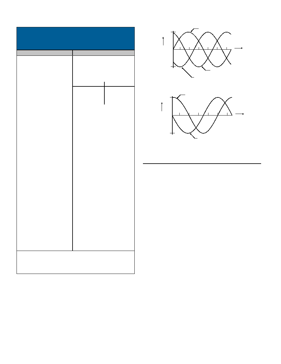
Standard Synchro Control Transmitter (CX) Outputs as a Function of CCW
Rotation From Electrical Zero (EZ).
Standard Resolver Control Transmitter (RX) Outputs as a Function of CCW
Rotation From Electrical Zero (EZ) With R2-R4 Excited.
FIGURE 2. SYNCHRO AND RESOLVER SIGNALS
INTRODUCTION
The circuit shown in FIGURE 1, the SD-14590/91/92 block dia-
gram, consists of three main parts: the signal input; a feedback
loop whose elements are the control transformer, demodulator,
error processor, VCO and up-down counter; and digital interface
circuitry including various latches and buffers.
SIGNAL INPUTS
The SD-14590/91/92 series offer three input options: synchro,
resolver, and direct. In a synchro or resolver mode, shaft angle
data is transmitted as the ratio of carrier amplitudes across the
input terminals. Synchro signals, which are of the form sin
θ
cos
ωt, sin(θ + 120°)cosωt, and sin(θ + 240°)cosωt are internally
converted to resolver format; sin
θcosωt and cosθcosωt. Direct
inputs accept 1 Vrms inputs in resolver form, (sin
θcosωt and
cos
θcosωt) and are buffered prior to conversion. FIGURE 2 illus-
trates synchro and resolver signals as a function of the angle
θ.
The solid-state signal and reference inputs are true differential
inputs with high AC and DC common mode rejection. Input
impedance is maintained with power off.
SOLID-STATE BUFFER INPUT PROTECTION:
TRANSIENT VOLTAGE SUPPRESSION
The solid-state signal and reference inputs are true differential
inputs with high AC and DC common rejection so most applica-
tions will not require units with isolation transformers. Input
impedance is maintained with power off. The current AC peak
+DC common mode voltage should not exceed the values in
TABLE 1.
90 V line-to-line systems may have voltage transients which
exceed the 500 V specification. These transients can destroy the
thin-film input resistor network in the hybrid. Therefore, 90 VL-L
solid-state input modules may be protected by installing voltage
suppressors as shown. Voltage transients are likely to occur
whenever synchro or resolver inputs are switched on and off. For
相關(guān)PDF資料 |
PDF描述 |
|---|---|
| SD-14591D1-394L | SYNCHRO OR RESOLVER TO DIGITAL CONVERTER, MDIP36 |
| SD-14551FX-412K | SYNCHRO OR RESOLVER TO DIGITAL CONVERTER, CDMA34 |
| SD-14596D2-284L | SYNCHRO OR RESOLVER TO DIGITAL CONVERTER, DIP36 |
| SD-14596D2-322Z | SYNCHRO OR RESOLVER TO DIGITAL CONVERTER, DIP36 |
| SD-14596D2-362 | SYNCHRO OR RESOLVER TO DIGITAL CONVERTER, DIP36 |
相關(guān)代理商/技術(shù)參數(shù) |
參數(shù)描述 |
|---|---|
| SD-14595D1-102 | 制造商:未知廠家 制造商全稱:未知廠家 功能描述:Synchro-to-Digital Converter |
| SD-14595D1-104 | 制造商:未知廠家 制造商全稱:未知廠家 功能描述:Synchro-to-Digital Converter |
| SD-14595D1-105 | 制造商:未知廠家 制造商全稱:未知廠家 功能描述:Synchro-to-Digital Converter |
| SD-14595D1-112 | 制造商:未知廠家 制造商全稱:未知廠家 功能描述:Synchro-to-Digital Converter |
| SD-14595D1-114 | 制造商:未知廠家 制造商全稱:未知廠家 功能描述:Synchro-to-Digital Converter |
發(fā)布緊急采購(gòu),3分鐘左右您將得到回復(fù)。