- 您現(xiàn)在的位置:買賣IC網(wǎng) > PDF目錄385839 > SF1103B (RF Monolithics, Inc.) 285 MHz SAW Filter PDF資料下載
參數(shù)資料
| 型號(hào): | SF1103B |
| 廠商: | RF Monolithics, Inc. |
| 英文描述: | 285 MHz SAW Filter |
| 中文描述: | 285兆赫SAW濾波器 |
| 文件頁(yè)數(shù): | 1/7頁(yè) |
| 文件大小: | 314K |
| 代理商: | SF1103B |
Preliminary
RF Monolithics, Inc.
RFM Europe
2001 by RF Monolithics, Inc. The stylized RFM logo are registered trademarks of RF Monolithics, Inc.
Phone: (972) 233-2903
Phone: 44 1963 251383
Fax: (972) 387-8148
Fax: 44 1963 251510
E-mail: info@rfm.com
http://www.rfm.com
SF1103B-121504
Page 1 of 4
Electrical Characteristics
Characteristic
Sym
f
C
IL
BW
1
BW
3
Notes
1
Min
Typ
Max
Units
MHz
dB
Nominal Center Frequency
Passband
285.000
14.5
±2.0
±2.5
0.8
Insertion Loss at fc
1 dB Passband
3 dB Passband
1, 2
TBD
mHz
Amplitude Ripple over fc±1.9 MHz
Group Delay Variation over fc±1.9 MHz
fc-25 to fc-5.0 and fc+5.0 to fc+25 MHz
1.0
dB
P-P
ns
P-P
dB
GDV
70
42
150
Rejection
Operating Temperature Range
1, 2, 3
40
T
A
1
-20
+80
°C
SMP-03
Designed for WCDMA 3G IF Applications
Quartz Temperature Stability
Small Size
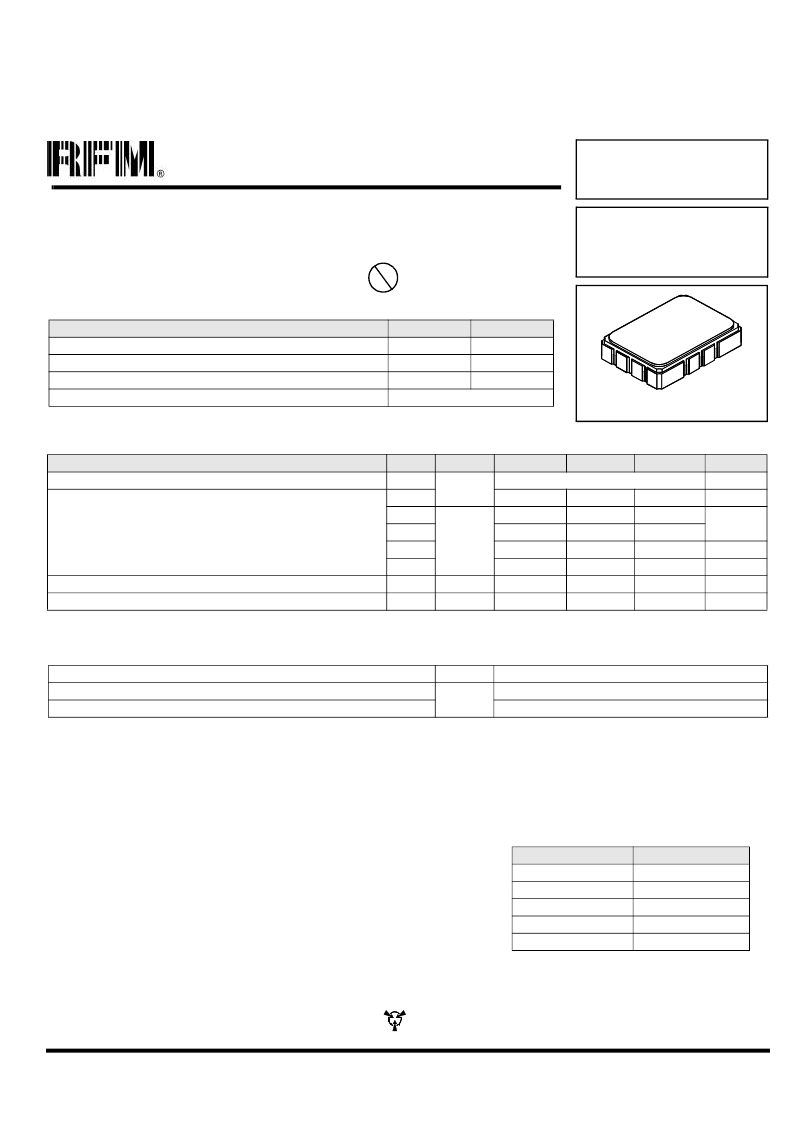
Hermetic 7 x 5 Surface-Mount Case
Complies with Directive 2002/95/EC (RoHS)
Absolute Maximum Ratings
Rating
Value
+10
30
-40 to +85
Units
dBm
VDC
°C
Maximum Incident Power in Passband
Max. DC voltage between any 2 terminals
Storage Temperature Range
Suitable for lead-free soldering - Max. Soldering Profile
265°C for 90 s
285 MHz
SAW Filter
SF1103B
Notes:
1.
Unless noted otherwise, all specifications apply over the operating temperature range
with filter soldered to the specified demonstration board with impedance matching to 50 W
and measured with 50
network analyzer.
Unless noted otherwise, all frequency specifications are referenced to the nominal center
frequency, fc.
Rejection is measured as attenuation below the minimum IL point in the passband.
Rejection in final user application is dependent on PCB layout and external impedance
matching design. See Application Note No. 42 for details.
"LRIP" or "L" after the part number indicates "low rate initial production" and "ENG" or "E"
indicates "engineering prototypes."
The design, manufacturing process, and specifications of this filter are subject to change.
Tape and Reel Standard ANSI / EIA 481.
Either Port 1 or Port 2 may be used for either input or output in the design. However,
impedances and impedance matching may vary between Port 1 and Port 2, so that the fil-
ter must always be installed in one direction per the circuit design.
US and international patents may apply.
Electrostatic Sensitive Device. Observe precautions for handling.
2.
3.
4.
5.
6.
7.
8.
9.
Connection
Port 1 Hot
Port 1 Gnd Return
Port 2 Hot
Port 2 Gnd Return
Case Ground
Terminals
10
1
5
6
All others
Electrical Connections
Matching to Unbalanced 50
Case Style
Lid Symbolization (YY = year, WW = week)
External L-C
6
SMP-03 7 x 5 mm Nominal Footprint
RFM SF1103A-1 YYWW
Pb
相關(guān)PDF資料 |
PDF描述 |
|---|---|
| SF1111A | 160 MHz SAW Filter |
| SF1114A-1 | 137.2 MHz SAW Filter |
| SF1120B | 298.74 MHz SAW Filter |
| SF1122A | 190 MHz SAW Filter |
| SF1124A | 190 MHz SAW Filter |
相關(guān)代理商/技術(shù)參數(shù) |
參數(shù)描述 |
|---|---|
| SF1104-6001 | 制造商:SOLICO 功能描述: |
| SF1105 6001 | 制造商: 功能描述: 制造商:undefined 功能描述: |
| SF1108-6001 | 制造商:SOLICO 功能描述: |
| SF110L | 制造商:VANLONG 制造商全稱:VANLONG 功能描述:110.00 MHz SAW Filter |
| SF110N | 制造商:VANLONG 制造商全稱:VANLONG 功能描述:110.592 MHz SAW Filter |
發(fā)布緊急采購(gòu),3分鐘左右您將得到回復(fù)。