- 您現(xiàn)在的位置:買賣IC網(wǎng) > PDF目錄48033 > SFH608-5-X017 (VISHAY SEMICONDUCTORS) 1 CHANNEL TRANSISTOR OUTPUT OPTOCOUPLER PDF資料下載
參數(shù)資料
| 型號: | SFH608-5-X017 |
| 廠商: | VISHAY SEMICONDUCTORS |
| 元件分類: | 光電耦合器 |
| 英文描述: | 1 CHANNEL TRANSISTOR OUTPUT OPTOCOUPLER |
| 封裝: | ROHS COMPLIANT, SMD, 4 PIN |
| 文件頁數(shù): | 2/8頁 |
| 文件大小: | 120K |
| 代理商: | SFH608-5-X017 |
www.vishay.com
For technical questions, contact: optocoupler.answers@vishay.com
Document Number: 83664
602
Rev. 1.5, 10-Dec-08
SFH608
Vishay Semiconductors
Optocoupler, Phototransistor Output,
Low Input Current, with Base
Connection, 5300 VRMS
Notes
(1) Tamb = 25 °C, unless otherwise specified.
Stresses in excess of the absolute maximum ratings can cause permanent damage to the device. Functional operation of the device is not
implied at these or any other conditions in excess of those given in the operational sections of this document. Exposure to absolute maximum
ratings for extended periods of the time can adversely affect reliability.
(2) Refer to reflow profile for soldering conditions for surface mounted devices (SMD). Refer to wave profile for soldering conditions for through
hole devices (DIP).
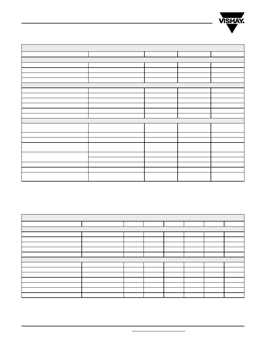
ABSOLUTE MAXIMUM RATINGS (1)
PARAMETER
TEST CONDITION
SYMBOL
VALUE
UNIT
INPUT
Reverse voltage
VR
6V
DC forward current
IF
50
mA
Surge forward current
tP ≤ 10 s
IFSM
2.5
A
Total power dissipation
Pdiss
70
mW
OUTPUT
Collector emitter voltage
VCE
55
V
Collector base voltage
VCBO
55
V
Emitter base voltage
VEBO
7V
Collector current
IC
50
mA
Surge collector current
tP ≤ 1.0 ms
100
mA
Total power dissipation
Pdiss
150
mW
COUPLER
Isolation test voltage
between emitter and detector
t = 1.0 s
VISO
5300
VRMS
Creepage distance
≥ 7mm
Clearance distance
≥ 7mm
Comparative tracking index per
DIN IEC 112/VDE0303, part 1
175
Isolation resistance
VIO = 500 V, Tamb = 25 °C
RIO
≥ 1012
Ω
VIO = 500 V, Tamb = 100 °C
RIO
≥ 1011
Ω
Storage temperature range
Tstg
- 55 to + 150
°C
Operating temperature range
Tamb
- 55 to + 100
°C
Soldering temperature (2)
max. 10 s, dip soldering: distance
to seating plane
≥ 1.5 mm
Tsld
260
°C
ELECTRICAL CHARACTERISTICS
PARAMETER
TEST CONDITION
PART
SYMBOL
MIN.
TYP.
MAX.
UNIT
INPUT
Forward voltage
IF = 5 mA
VF
1.1
1.5
V
Reverse voltage
IR = 10 A
VR
6V
Reverse current
VR = 6 V
IR
0.01
10
A
Capacitance
VR = 0 V, f = 1 MHz
CO
25
pF
Thermal resistance
Rthja
1070
K/W
OUTPUT
Collector emitter voltage
ICE = 10 A
VCEO
55
V
Emitter base voltage
IEB = 10 A
VEBO
7V
Collector emitter capacitance
VCE = 5 V, f = 1 MHz
CCE
10
pF
Collector base capacitance
VCE = 5 V, f = 1 MHz
CCB
16
pF
Emitter base capacitance
VCE = 5 V, f = 1 MHz
CEB
10
pF
Thermal resistance
Rthja
500
K/W
Collector emitter leakage current
VCE = 10 V
ICEO
10
200
nA
相關(guān)PDF資料 |
PDF描述 |
|---|---|
| SFH608-2-X009 | 1 CHANNEL TRANSISTOR OUTPUT OPTOCOUPLER |
| SFH608-2-X019 | 1 CHANNEL TRANSISTOR OUTPUT OPTOCOUPLER |
| SFH608-3-X007 | 1 CHANNEL TRANSISTOR OUTPUT OPTOCOUPLER |
| SFH608-5 | 1 CHANNEL TRANSISTOR OUTPUT OPTOCOUPLER |
| SFH608-2-X016 | 1 CHANNEL TRANSISTOR OUTPUT OPTOCOUPLER |
相關(guān)代理商/技術(shù)參數(shù) |
參數(shù)描述 |
|---|---|
| SFH609 | 制造商:INFINEON 制造商全稱:Infineon Technologies AG 功能描述:HIGH RELIABILITY PHOTOTRANSISTOR OPTOCOUPLER |
| SFH609-1 | 制造商:ISOCOM 制造商全稱:ISOCOM 功能描述:OPTICALLY COUPLED ISOLATOR PHOTOTRANSISTOR OUTPUT |
| SFH609-2 | 制造商:ISOCOM 制造商全稱:ISOCOM 功能描述:OPTICALLY COUPLED ISOLATOR PHOTOTRANSISTOR OUTPUT |
| SFH609-3 | 制造商:未知廠家 制造商全稱:未知廠家 功能描述:OPTICALLY COUPLED ISOLATOR PHOTOTRANSISTOR OUTPUT |
| SFH609-4 | 制造商:未知廠家 制造商全稱:未知廠家 功能描述:OPTICALLY COUPLED ISOLATOR PHOTOTRANSISTOR OUTPUT |
發(fā)布緊急采購,3分鐘左右您將得到回復(fù)。