- 您現(xiàn)在的位置:買賣IC網(wǎng) > PDF目錄376345 > SG1526BJ (MICROSEMI CORP-ANALOG MIXED SIGNAL GROUP) REGULATING PULSE WIDTH MODULATOR PDF資料下載
參數(shù)資料
| 型號(hào): | SG1526BJ |
| 廠商: | MICROSEMI CORP-ANALOG MIXED SIGNAL GROUP |
| 元件分類: | 穩(wěn)壓器 |
| 英文描述: | REGULATING PULSE WIDTH MODULATOR |
| 中文描述: | 0.2 A SWITCHING CONTROLLER, 500 kHz SWITCHING FREQ-MAX, CDIP18 |
| 封裝: | HERMETIC SEALED, CERAMIC, DIP-18 |
| 文件頁數(shù): | 7/9頁 |
| 文件大小: | 209K |
| 代理商: | SG1526BJ |

4/90 Rev 1.1 2/94
Copyright
1994
L
IN
F
IN
ITY
Microelectronics Inc.
11861 Western Avenue
∞
∞
Garden Grove, CA 92841
(714) 898-8121
∞
FAX: (714) 893-2570
7
SG1526B/SG2526B/SG3526B
APPLICATION INFORMATION
(continued)
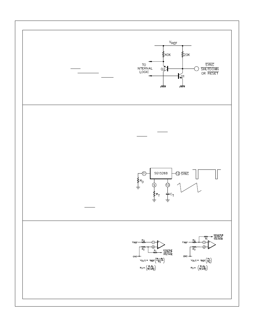
DIGITAL CONTROL PORTS
The three digital control ports of the SG1526B are bi-
directional. Each pin can drive TTL and 5 volt CMOS logic
directly, up to a fan-out of 10 low-power Schottky gates.
Each pin can also be directly driven by open-collector TTL,
open-drain CMOS, and open-collector voltage comparators,
fan-in is equivalent to 1 low-power Schottky gate. Each port
is normally HIGH; the pin is pulled LOW to activate the
particular function. Driving SYNC LOW initiates a discharge
cycle in the oscillator. Pulling SHUTDOWN LOW immedi-
ately inhibits all PWM output pulses. Holding RESET LOW
discharges the soft-start capacitor. The logic threshold is
+1.1 volts at +25
o
C. Noise immunity can be gained at the
expense of fan-out with an external 2K pull-up resistor to +5
volts.
OSCILLATOR
The oscillator is programmed for frequency and dead time
with three components: R
C
, and R
. Two waveforms are
generated: a sawtooth waveform at pin 10 for pulse width
modulation, and a logic clock at pin 12. The following
procedure is recommended for choosing timing values:
1. With R
= 0
(pin 11 shorted to ground) select values
for R
and C
from Figure 19 to give the desired
oscillator period. Remember that the frequency at
each driver output is half the oscillator frequency, and
the frequency at the +V
C
terminal is the same as the
oscillator frequency.
2. If more dead time is required, select a larger value of
R
using Figure 14 as a guide. At 40 KHz dead time
increases by 300 ns/
.
3. Increasing the dead time will cause the oscillator
frequency to decrease slightly. Go back and de-
crease the value of R
slightly to bring the frequency
back to the nominal design value.
The SG1526B can be synchronized to an external logic clock
by programming the oscillator to free-run at a frequency 10%
slower than the sync frequency. A periodic LOW logic pulse
approximately 0.5
μ
Sec wide at the SYNC pin will then lock
the oscillator to the external frequency.
Multiple devices can be synchronized together by program-
ming one master unit for the desired frequency, and then
sharing its sawtooth and clock waveforms with the slave
units. All C
terminals are connected to the C
pin of the
master, and all SYNC terminals are likewise connected to
the SYNC pin of the master. Slave R
terminals should not
be left open; at least 50K should be connected from each pin
to ground. Slave R
D
terminals may be either left open or
grounded.
FIGURE 24.
OSCILLATOR CONNECTIONS ANDD WAVEFORMS
ERROR AMPLIFIER
The error amplifier is a transconductance design, with an
output impedance of 2 megohms. Since all voltage gain
takes place at the output pin, the open-loop gain/frequency
characteristics can be controlled with shunt reactance to
ground. When compensated for unity-gain stability with 100
pF, the amplifier has an open-loop pole at 400 Hz.
The input connections to the error amplifier and determined
by the polarity of the switching supply output voltage. For
positive supplies, the common-mode voltage is +5.0 volts
and the feedback connections in Figure 25A are used. With
negative supplies, the common-mode voltage is ground and
the feedback divider is connected between the negative
output and the +5.0 volt reference voltage, as shown in
Figure 25B.
FIGURE 25.
ERROR AMPLIFIER CONNECTIONS
FIGURE 23
DIGITAL CONTROL PORT SCHEMATIC
(A)
(B)
相關(guān)PDF資料 |
PDF描述 |
|---|---|
| SG1526BL | CAP .012UF 250V PEN FILM 1913 5% |
| SG3526B | REGULATING PULSE WIDTH MODULATOR |
| SG3526BDW | REGULATING PULSE WIDTH MODULATOR |
| SG3526BJ | REGULATING PULSE WIDTH MODULATOR |
| SG3526BN | REGULATING PULSE WIDTH MODULATOR |
相關(guān)代理商/技術(shù)參數(shù) |
參數(shù)描述 |
|---|---|
| SG1526BJ/883B | 制造商:Microsemi Corporation 功能描述:Voltage Mode PWM Controller 100mA 18-Pin CDIP |
| SG1526BJ/DESC | 制造商:MICROSEMI 制造商全稱:Microsemi Corporation 功能描述:REGULATING PULSE WIDTH MODULATOR |
| SG1526BJ/JAN | 制造商:Microsemi Corporation 功能描述:Voltage Mode PWM Controller 100mA 18-Pin CDIP |
| SG1526BJ-883B | 制造商:Microsemi Corporation 功能描述:Voltage Mode PWM Controller 100mA 18-Pin CDIP 制造商:Microsemi Corporation 功能描述:VOLT MODE PWM CNTRLR 100MA 18CDIP - Rail/Tube 制造商:Microsemi Corporation 功能描述:IC REG CTRLR BUCK PWM VM 18JDIP |
| SG1526BJ-DESC | 制造商:Microsemi Corporation 功能描述:Voltage Mode PWM Controller 100mA 18-Pin CDIP 制造商:Microsemi Corporation 功能描述:VOLT. MODE PWMS - Rail/Tube 制造商:Microsemi Corporation 功能描述:IC REG CTRLR BUCK PWM VM 18JDIP |
發(fā)布緊急采購(gòu),3分鐘左右您將得到回復(fù)。