- 您現(xiàn)在的位置:買賣IC網(wǎng) > PDF目錄376348 > SG3731 (Microsemi Corporation) DC MOTOR PULSE WIDTH MODULATOR PDF資料下載
參數(shù)資料
| 型號: | SG3731 |
| 廠商: | Microsemi Corporation |
| 英文描述: | DC MOTOR PULSE WIDTH MODULATOR |
| 中文描述: | 直流電機脈寬調(diào)制器 |
| 文件頁數(shù): | 3/5頁 |
| 文件大?。?/td> | 140K |
| 代理商: | SG3731 |

SG1731/SG2731/SG3731
4/90 Rev 1.3 9/99
Copyright
1999
L
IN
F
IN
ITY
Microelectronics Inc.
Garden
Grove,
FAX: (714) 893-2570
11861 Western Avenue
∞
CA
92841
3
(714) 898-8121
∞
ELECTRICAL CHARACTERISTICS
(continued)
Test Conditions
Units
Min.
Typ. Max.
SHUTDOWN Section
Logic Threshold
SHUTDOWN HIGH Current
SHUTDOWN LOW Current
Output Drivers (Each Output)
Parameter
SG1731/2731/3731
HIGH Output Voltage
LOW Output Voltage
Driver Risetime
Driver Falltime
Total Supply Current
V
S
Supply Current
V
O
Supply Current
APPLICATION INFORMATION
The SG1731 requires a supply voltage for the control circuitry (V
S
)
and for the power output drivers (V
). Each supply may be either
balanced positive and negative with respect to ground, or single-
ended. The only restrictions are:
1.The voltage between +V
S
and -V
S
must be at least 7.0V; but
no more than 44V.
2.The voltage between +V
O
and -V
O
must be at least 5.0V; but
no more than 44V.
3.+V
must be at least 5V more positive than -V
. This
eliminates the combination of a single-ended positive control
supply with a single-ended negative driver supply.
SUBSTRATE CONNECTION
The substrate connection (Pin 10) must always be connected to
either -V
or -V
, whichever is more negative. The substrate must
also be well bypassed to ground with a high quality capacitor.
OSCILLATOR
The triangle oscillator consists of two voltage comparators, a set/
reset flip-flop, a bi-directional 500
μ
A current source, and an
external timing capacitor C
. A positive reference voltage (2V
+
)
applied to Pin 2 determines the positive peak value of the triangle,
and a negative reference voltage (2V
-
) at Pin 7 sets the negative
peak value of the triangle waveform.
Since the value of the internal current source is fixed at a nominal
±500
μ
A, the oscillator period is a function of the selected peak-
to-peak voltage excursion and the value of C
T
. The theoretical
expression for the oscillator period is:
T
OSC
=
(Eq.1)
where C
is the timing capacitor in Farads and dV is V
OSC
in Volts
peak-to-peak.
ERROR AMPLIFIER
The error amplifier of the SG1731 is a conventional internally-
compensated operational amplifier with low output impedance.
All of the usual feedback and frequency compensation
techniques may be use to control the closed-loop gain
characteristics. The control supply voltage ±V
will determine the
input common mode range and output voltage swing; both will
extend to within 3V of the V
S
supply.
PULSE WIDTH MODULATION
Pulse width modulation occurs by comparing the triangle
waveform to a fixed upper (+V
) and lower (-V
) threshold
voltage. A crossing above the upper threshold causes
Output A to switch to the HIGH state, and a crossing below
-V
S
= -3.5V to -15V
V
SHUTDOWN
= -V
S
+2.4V
V
SHUTDOWN
= -V
S
Note 3. These parameters, although guaranteed, are not tested in production.
Note 4. Unity Gain Inverting 10K
Feedback Resistance.
Note 5. V
CM
=
±
12V.
2C
T
dV
5 x 10
-4
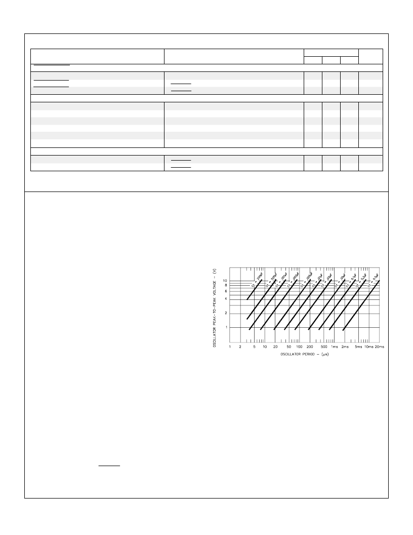
As a design aid, the solutions to Equation 1 over the
recommended range of T
and V
are given in graphic form in
Figure 1. The lower limit on T
is 1.85
μ
s, corresponding to a
maximum frequency of 350 KHz. The maximum value of V
OSC
,
(2V
+
) - (2V
-
), is 10V peak-to-peak for linear waveforms.
FIGURE 1 - SG1731 OSCILLATOR PERIOD VS. V
OSC
AND C
T
V
+2.0
400
-1.0
V
S
+0.8
V
μ
A
mA
I
SOURCE
= 20mA
I
SOURCE
= 100mA
I
SINK
I
SINK
= 100mA
C
L
= 1000pF
C
L
= 1000pF
V
V
V
V
ns
ns
19.2
19.0
-19.2
-19.0
300
300
14
6
mA
mA
V
SHUTDOWN
= -V
S
+ 0.8V
V
SHUTDOWN
= -V
S
+ 0.8V
相關PDF資料 |
PDF描述 |
|---|---|
| SG3731J | DC MOTOR PULSE WIDTH MODULATOR |
| SG3731N | DC MOTOR PULSE WIDTH MODULATOR |
| SG2731N | DC MOTOR PULSE WIDTH MODULATOR |
| SG1731 | DC MOTOR PULSE WIDTH MODULATOR |
| SG1731J | DC MOTOR PULSE WIDTH MODULATOR |
相關代理商/技術參數(shù) |
參數(shù)描述 |
|---|---|
| SG3731J | 制造商:Microsemi Corporation 功能描述:DC MOTOR DRVR 3.5V TO 15V/-15V TO -3.5V 16CDIP - Bulk |
| SG3731N | 制造商:Microsemi Corporation 功能描述:DC MOTOR DRVR 3.5V TO 15V/-15V TO -3.5V 16PDIP - Bulk |
| SG374 | 制造商:Distributed By MCM 功能描述:16 Port Cat6 Rack Mount Patch Panel |
| SG375 | 制造商:Distributed By MCM 功能描述:24 Port Cat6 Rack Mount Patch Panel |
| SG375500D-24 | 功能描述:EMI 連接器墊圈 D Shape RFI Shielding Gasket RoHS:否 制造商:FerriShield 連接器類型: 外殼大小: 厚度:6.35 mm 等級: |
發(fā)布緊急采購,3分鐘左右您將得到回復。