- 您現(xiàn)在的位置:買賣IC網(wǎng) > PDF目錄373391 > SG6513 (Electronic Theatre Controls, Inc.) PC Power Supply Supervisors PDF資料下載
參數(shù)資料
| 型號(hào): | SG6513 |
| 廠商: | Electronic Theatre Controls, Inc. |
| 英文描述: | PC Power Supply Supervisors |
| 中文描述: | PC電源監(jiān)控 |
| 文件頁(yè)數(shù): | 7/11頁(yè) |
| 文件大小: | 227K |
| 代理商: | SG6513 |
Product
Specification
PC Power Supply Supervisors
SG6513/T
System General Corp.
Version 1.0PN ( IRO33.0014.B0)
- 7 -
www.sg.com.tw
Aug.26,2003
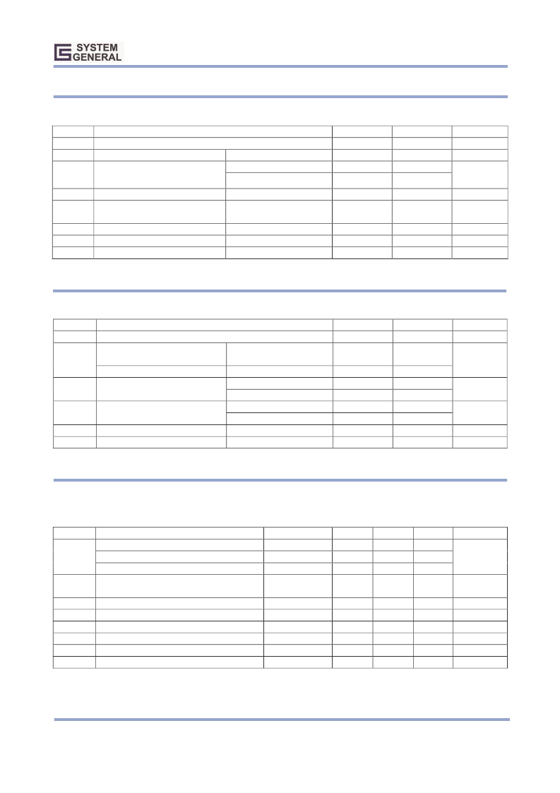
ABSOLUTE MAXIMUM RATINGS
Symbol Parameter
V
DD
DC Supply Voltage
V
I
Input Voltage
Min.
-0.3
-0.3
-0.3
Max.
16
8
16
Unit
V
V
PSON, VS33, VS5, PGI
FPO
V
OUT
Output Voltage
PGO
-0.3
8
V
P
D
Power Dissipation
400
mW
T
A
Operating Free Air Temperature
Range
Storage Temperature Range
Soldering Temperature
ESD Capability, HBM model
-40
85
℃
T
STG
-55
150
260
5
℃
℃
KV
Note: Stresses above those listed may cause permanent damage to the device.
RECOMMENDED OPERATING CONDITIONS
Symbol
Parameter
V
DD
DC Supply Voltage
Min.
4
Max.
15
Unit
V
Input Voltage
PSON, VS33, VS5, IS33, IS5,
PGI
VS12, IS12
FPO
PGO
FPO
PGO
See Note
7
V
I
Input Voltage
1
12.5
15
15
7
20
10
62.5
V
V
OUT
Output Voltage
V
I
OSINK
Output Sink Current
mA
T
R
I
RI
Supply Voltage Rising Time
Output Current RI
mS
uA
Note: VDD rising and falling slew rate must be less than 14V/mS.
ELECTRICAL CHARACTERISTICS (VDD=12V, TA=25
℃
)
Over-voltage and Over-current Protection
Symbol Parameter
Over-voltage Protection VS33
Over-voltage Protection VS5
V
OVP
Over-voltage Protection VS12
Ratio of current sense sink current to current
sense setting pin (RI) source current
V
OFFSET
OCP comparator input offset voltage
I
LKG
Leakage Current (FPO)
V
OL
Low Level Output Voltage (FPO)
T
OVP
Timing OVP to Protection
T
OCP
Timing OCP to Protection
V
RI
Current Source Reference Voltage
Test Conditions Min.
RI = 30
Κ,
0.1% Resistor
V(FPO) = 5V
Isink 20mA
Typ.
4.1
6.1
13.8
Max.
4.3
6.5
14.4
Unit
3.9
5.7
13.2
V
I
REF
7.6
8
8.4
-5
33
75
1.1
75
125
1.15
5
5
0.7
110
175
1.2
mV
uA
V
uS
uS
V
相關(guān)PDF資料 |
PDF描述 |
|---|---|
| SG6513D | PC Power Supply Supervisors |
| SG6513S | PC Power Supply Supervisors |
| SG6513T | PC Power Supply Supervisors |
| SG6513TD | PC Power Supply Supervisors |
| SG6513TS | PC Power Supply Supervisors |
相關(guān)代理商/技術(shù)參數(shù) |
參數(shù)描述 |
|---|---|
| SG6513D | 制造商:未知廠家 制造商全稱:未知廠家 功能描述:PC Power Supply Supervisors |
| SG6513S | 制造商:未知廠家 制造商全稱:未知廠家 功能描述:PC Power Supply Supervisors |
| SG6513T | 制造商:未知廠家 制造商全稱:未知廠家 功能描述:PC Power Supply Supervisors |
| SG6513TD | 制造商:未知廠家 制造商全稱:未知廠家 功能描述:PC Power Supply Supervisors |
| SG6513TS | 制造商:未知廠家 制造商全稱:未知廠家 功能描述:PC Power Supply Supervisors |
發(fā)布緊急采購(gòu),3分鐘左右您將得到回復(fù)。