- 您現(xiàn)在的位置:買賣IC網(wǎng) > PDF目錄373395 > Si5023-BM (Electronic Theatre Controls, Inc.) MULTI-RATE SONET/SDH CDR IC WITH LIMITING AMP PDF資料下載
參數(shù)資料
| 型號: | Si5023-BM |
| 廠商: | Electronic Theatre Controls, Inc. |
| 元件分類: | 運動控制電子 |
| 英文描述: | MULTI-RATE SONET/SDH CDR IC WITH LIMITING AMP |
| 中文描述: | 多速率SONET / SDH的CDR集成電路限幅放大器 |
| 文件頁數(shù): | 14/22頁 |
| 文件大小: | 399K |
| 代理商: | SI5023-BM |
Si5022/Si5023
14
Preliminary Rev. 0.46
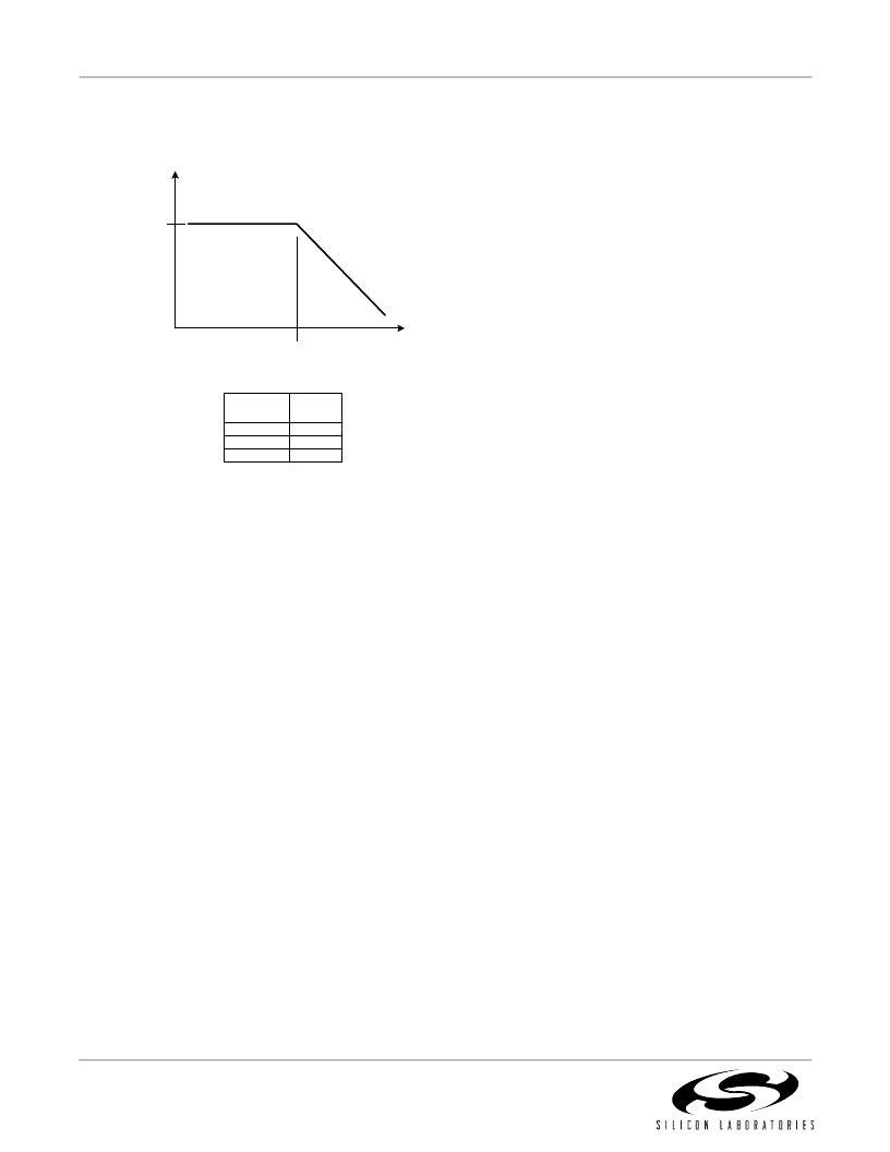
test signal that is degraded with sinusoidal jitter whose
magnitude is defined by the mask in Figure 9.
Figure 9. Jitter Transfer Specification
Jitter Generation
The Si5022/23 exceeds all relevant specifications for
jitter generation proposed for SONET/SDH equipment.
The jitter generation specification defines the amount of
jitter that may be present on the recovered clock and
data outputs when a jitter free input signal is provided.
The
Si5022/23
typically
3.0 mUI
RMS
of jitter when presented with jitter-free input
data.
RESET/DSPLL Calibration
The Si5022/23 achieves optimal jitter performance by
using self-calibration circuitry to set the loop gain
parameters within the DSPLL. For the self-calibration
circuitry to operate correctly, the power supply voltage
must exceed TBD V when calibration occurs. Self-
calibration is initiated by a high-to-low transition on the
RESET/CAL pin. The RESET/CAL pin must be held
high for at least 1
μ
S after the supply has stabilized on
power-up for optimum device operation. When RESET/
CAL is released (set to low) the digital logic resets to a
known initial condition, recalibrates the DSPLL, and will
begin to lock to the incoming data stream.
Clock Disable
The
Si5022/23
provides
CLK_DSBL, that is used to disable the recovered clock
output, CLKOUT. When the CLK_DSBL pin is asserted,
the positive and negative terminals of CLKOUT are tied
to VDD through 100
on-chip resistors. This feature is
generates
less
than
a
clock
disable
pin,
used to reduce power consumption in applications that
do not use the recovered clock.
Data Squelch
The Si5022/23 provides a data squelching pin,
DSQLCH, that is used to set the recovered data output,
DOUT, to binary zero. When the DSQLCH pin is
asserted, the DOUT logic signal is held at a binary zero.
This pin can be is used to squelch corrupt data during
LOS and LOL situations. Care must be taken when ac
coupling these outputs; a long string of zeros will not be
held through ac coupling capacitors.
Device Grounding
The Si5022/23 uses the GND pad on the bottom of the
28-pin micro leaded package (MLP) for device ground.
This pad should be connected directly to the analog
supply ground. See Figures 13 and 14 for the ground
(GND) pad location.
Bias Generation Circuitry
The Si5022/23 makes use of an external resistor to set
internal bias currents. The external resistor allows
precise generation of bias currents which significantly
reduces
power
consumption
implementations that use an internal resistor. The bias
generation circuitry requires a 10 k
(1%) resistor
connected between REXT and GND.
Voltage Regulator
The Si5022 and Si5023 operate from different external
supply voltages. Internally the devices are identical and
operate from a 2.5 V supply. The Si5022 takes the 2.5 V
supply directly from the external supply connections.
The Si5023 regulates 2.5 V internally down from the
external 3.3 V supply. Both devices consume 148 mA
typically.
In addition to supporting 3.3 V systems, the on-chip
linear regulator offers better power supply noise
rejection versus the direct 2.5 V supply.
Differential Input Circuitry
The Si5022/23 provides differential inputs for both the
high speed data (DIN) and the reference clock
(REFCLK) inputs. An example termination for these
inputs is shown in Figure 10 and Figure 11 respectively.
In applications where direct dc coupling is possible, the
0.1
μ
F capacitors may be omitted. (LOS operation is
only guaranteed when ac coupled.) The data input
limiting amplifier requires an input signal with a
differential peak-to-peak voltage as specified in Table 2
to ensure a BER of at least 10
–12
. The REFCLK input
differential
peak-to-peak
specified in Table 2.
versus
traditional
voltage
requirement
is
0.1 dB
Jitter
Transfer
Fc
Frequency
20 dB/Decade
Slope
Fc
(kHz)
2000
500
130
SONET
Data Rate
OC-48
OC-12
OC-3
Acceptable
Range
相關PDF資料 |
PDF描述 |
|---|---|
| SI5022 | MULTI-RATE SONET/SDH CDR IC WITH LIMITING AMP |
| SI5311 | PRECISION HIGH SPEED CLOCK MULTIPLIER/REGENERATOR IC |
| SI5311-BM | BAIL MOUNT/100 BULK PKG |
| SI5312-H(B) | IRED |
| SI5312-H | IRED |
相關代理商/技術參數(shù) |
參數(shù)描述 |
|---|---|
| SI5023-BMR | 功能描述:時鐘合成器/抖動清除器 SNT/SDH GbE 2.7Gbps OC48/12/3 STM16/4/1 RoHS:否 制造商:Skyworks Solutions, Inc. 輸出端數(shù)量: 輸出電平: 最大輸出頻率: 輸入電平: 最大輸入頻率:6.1 GHz 電源電壓-最大:3.3 V 電源電壓-最小:2.7 V 封裝 / 箱體:TSSOP-28 封裝:Reel |
| Si5023-D-GM | 功能描述:時鐘合成器/抖動清除器 SNT/SDH GbE 2.7Gbps OC48/12/3 STM16/4/1 RoHS:否 制造商:Skyworks Solutions, Inc. 輸出端數(shù)量: 輸出電平: 最大輸出頻率: 輸入電平: 最大輸入頻率:6.1 GHz 電源電壓-最大:3.3 V 電源電壓-最小:2.7 V 封裝 / 箱體:TSSOP-28 封裝:Reel |
| SI5023-D-GMR | 功能描述:時鐘合成器/抖動清除器 Limiting amp 3.3 V RoHS:否 制造商:Skyworks Solutions, Inc. 輸出端數(shù)量: 輸出電平: 最大輸出頻率: 輸入電平: 最大輸入頻率:6.1 GHz 電源電壓-最大:3.3 V 電源電壓-最小:2.7 V 封裝 / 箱體:TSSOP-28 封裝:Reel |
| SI5023-EVB | 功能描述:時鐘和定時器開發(fā)工具 SNT/SDH GbE 2.7Gbps OC48/12/3 STM16/4/1 RoHS:否 制造商:Texas Instruments 產(chǎn)品:Evaluation Modules 類型:Clock Conditioners 工具用于評估:LMK04100B 頻率:122.8 MHz 工作電源電壓:3.3 V |
| SI5023-X-GM | 制造商:Silicon Laboratories Inc 功能描述: |
發(fā)布緊急采購,3分鐘左右您將得到回復。