- 您現(xiàn)在的位置:買賣IC網(wǎng) > PDF目錄373435 > SN54ABT845 (Texas Instruments, Inc.) Octal Bus Interface D-Type Latches With 3-State Outputs(八總線接口D鎖存器(三態(tài)輸出)) PDF資料下載
參數(shù)資料
| 型號: | SN54ABT845 |
| 廠商: | Texas Instruments, Inc. |
| 英文描述: | Octal Bus Interface D-Type Latches With 3-State Outputs(八總線接口D鎖存器(三態(tài)輸出)) |
| 中文描述: | 八路總線接口D類鎖存器與三態(tài)輸出(八總線接口?鎖存器(三態(tài)輸出)) |
| 文件頁數(shù): | 1/7頁 |
| 文件大小: | 117K |
| 代理商: | SN54ABT845 |
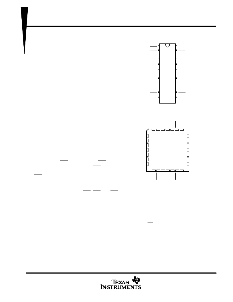
SN54ABT845 . . . JT PACKAGE
SN74ABT845 . . . DW OR NT PACKAGE
(TOP VIEW)
SN54ABT845 . . . FK PACKAGE
(TOP VIEW)
1
2
3
4
5
6
7
8
9
10
11
12
24
23
22
21
20
19
18
17
16
15
14
13
OE1
OE2
1D
2D
3D
4D
5D
6D
7D
8D
CLR
GND
V
CC
OE3
1Q
2Q
3Q
4Q
5Q
6Q
7Q
8Q
PRE
LE
NC – No internal connection
3 2 1 28 27
12 13
5
6
7
8
9
10
11
25
24
23
22
21
20
19
2Q
3Q
4Q
5Q
NC
6Q
7Q
2D
3D
4D
5D
NC
6D
7D
4
26
14 15 16 1718
8
C
G
N
L
P
8
1
O
O
N
O
1
V
C
C
SN54ABT845, SN74ABT845
OCTAL BUS INTERFACE D-TYPE LATCHES
WITH 3-STATE OUTPUTS
SCBS169 – FEBRUARY 1991–REVISED OCTOBER 1992
POST OFFICE BOX 655303
DALLAS, TEXAS 75265
Copyright
1992, Texas Instruments Incorporated
1
State-of-the-Art EPIC-
ΙΙ
B
BiCMOS Design
Significantly Reduces Power Dissipation
ESD Protection Exceeds 2000 V Per
MIL-STD-883C, Method 3015; Exceeds
200 V Using Machine Model (C = 200 pF,
R = 0)
Latch-Up Performance Exceeds 500 mA Per
JEDEC Standard JESD-17
Typical V
OLP
(Output Ground Bounce) < 1 V
at V
CC
= 5 V, T
A
= 25
°
C
High-Drive Outputs (–32-mA I
OH
,
64-mA I
OL
)
Package Options Include Plastic
Small-Outline Packages, Ceramic Chip
Carriers, and Standard Plastic and Ceramic
300-mil DIPs
description
The ’ABT845 9-bit latch is designed specifically for
driving
highly
capacitive
low-impedance loads. It is particularly suitable for
implementing
buffer
bidirectional bus drivers, and working registers.
or
relatively
registers,
I/O
ports,
The eight latches are transparent D-type latches.
The device has noninverting data (D) inputs and
provides true data at its outputs.
Since clear (CLR) and preset (PRE) are
independent of the clock, taking the CLR input low
causes the eight Q outputs to go low. Taking the
PRE input low will cause the eight Q outputs to go
high. When both PRE and CLR are taken low, the
outputs go high.
The buffered output-enable (OE1, OE2, and OE3) inputs can be used to place the eight outputs in either a
normal logic state (high or low levels) or a high-impedance state. In the high-impedance state, the outputs
neither load nor drive the bus lines significantly. The high-impedance state and increased drive provide the
capability to drive bus lines without need for interface or pullup components.
The output-enable inputs do not affect the internal operations of the latch. Previously stored data can be retained
or new data can be entered while the outputs are in the high-impedance state.
To ensure the high-impedance state during power up or power down, OE should be tied to V
CC
through a pullup
resistor; the minimum value of the resistor is determined by the current-sinking capability of the driver.
The SN54ABT845 is characterized for operation over the full military temperature range of –55
°
C to 125
°
C. The
SN74ABT845 is characterized for operation from –40
°
C to 85
°
C.
EPIC-
ΙΙ
B is a trademark of Texas Instruments Incorporated.
PRODUCT PREVIEW information concerns products in the formative or
design phase of development. Characteristic data and other
specifications are design goals. Texas Instruments reserves the right to
change or discontinue these products without notice.
P
相關(guān)PDF資料 |
PDF描述 |
|---|---|
| SN74ABT845 | Octal Bus Interface D-Type Latches With 3-State Outputs(八總線接口D觸發(fā)器(三態(tài)輸出)) |
| SN54ABT8543FK | SCAN TEST DEVICES WITH OCTAL REGISTERED BUS TRANSCEIVERS |
| SN54ABT8543JT | SCAN TEST DEVICES WITH OCTAL REGISTERED BUS TRANSCEIVERS |
| SN54ABT854 | 8-Bit To 9-Bit Parity Bus Transceivers(8-9奇偶總線收發(fā)器) |
| SN74ABT854 | 8-Bit To 9-Bit Parity Bus Transceivers(8-9奇偶總線收發(fā)器) |
相關(guān)代理商/技術(shù)參數(shù) |
參數(shù)描述 |
|---|---|
| SN54ABT853 | 制造商:TI 制造商全稱:Texas Instruments 功能描述:8-BIT TO 9-BIT PARITY BUS TRANSCEIVERS |
| SN54ABT853FK | 制造商:TI 制造商全稱:Texas Instruments 功能描述:8-BIT TO 9-BIT PARITY BUS TRANSCEIVERS |
| SN54ABT853JT | 制造商:TI 制造商全稱:Texas Instruments 功能描述:8-BIT TO 9-BIT PARITY BUS TRANSCEIVERS |
| SN54ABT853W | 制造商:TI 制造商全稱:Texas Instruments 功能描述:8-BIT TO 9-BIT PARITY BUS TRANSCEIVERS |
| SN54ABT8543 | 制造商:TI 制造商全稱:Texas Instruments 功能描述:SCAN TEST DEVICES WITH OCTAL REGISTERED BUS TRANSCEIVERS |
發(fā)布緊急采購,3分鐘左右您將得到回復(fù)。