- 您現(xiàn)在的位置:買賣IC網(wǎng) > PDF目錄98090 > SN7400DR (TEXAS INSTRUMENTS INC) TTL/H/L SERIES, QUAD 2-INPUT NAND GATE, PDSO14 PDF資料下載
參數(shù)資料
| 型號(hào): | SN7400DR |
| 廠商: | TEXAS INSTRUMENTS INC |
| 元件分類: | 門電路 |
| 英文描述: | TTL/H/L SERIES, QUAD 2-INPUT NAND GATE, PDSO14 |
| 封裝: | GREEN, PLASTIC, MS-012AB, SOIC-14 |
| 文件頁(yè)數(shù): | 18/23頁(yè) |
| 文件大?。?/td> | 804K |
| 代理商: | SN7400DR |
第1頁(yè)第2頁(yè)第3頁(yè)第4頁(yè)第5頁(yè)第6頁(yè)第7頁(yè)第8頁(yè)第9頁(yè)第10頁(yè)第11頁(yè)第12頁(yè)第13頁(yè)第14頁(yè)第15頁(yè)第16頁(yè)第17頁(yè)當(dāng)前第18頁(yè)第19頁(yè)第20頁(yè)第21頁(yè)第22頁(yè)第23頁(yè)
SN5400, SN54LS00, SN54S00
SN7400, SN74LS00, SN74S00
QUADRUPLE 2INPUT POSITIVENAND GATES
SDLS025B DECEMBER 1983 REVISED OCTOBER 2003
4
POST OFFICE BOX 655303
DALLAS, TEXAS 75265
absolute maximum ratings over operating free-air temperature (unless otherwise noted)
Supply voltage, VCC (see Note 1)
7 V
. . . . . . . . . . . . . . . . . . . . . . . . . . . . . . . . . . . . . . . . . . . . . . . . . . . . . . . . . . . . .
Input voltage: ’00, ’S00
5.5 V
. . . . . . . . . . . . . . . . . . . . . . . . . . . . . . . . . . . . . . . . . . . . . . . . . . . . . . . . . . . . . . . . . . . .
’LS00
7 V
. . . . . . . . . . . . . . . . . . . . . . . . . . . . . . . . . . . . . . . . . . . . . . . . . . . . . . . . . . . . . . . . . . . . . . . . .
Package thermal impedance,
θJA (see Note 2): D package
86
°C/W
. . . . . . . . . . . . . . . . . . . . . . . . . . . . . . . . . . .
DB package
96
°C/W
. . . . . . . . . . . . . . . . . . . . . . . . . . . . . . . . .
N package
80
°C/W
. . . . . . . . . . . . . . . . . . . . . . . . . . . . . . . . . . .
NS package
76
°C/W
. . . . . . . . . . . . . . . . . . . . . . . . . . . . . . . . .
PS package
95
°C/W
. . . . . . . . . . . . . . . . . . . . . . . . . . . . . . . . .
Storage temperature range, Tstg
65
°C to 150°C
. . . . . . . . . . . . . . . . . . . . . . . . . . . . . . . . . . . . . . . . . . . . . . . . . .
Stresses beyond those listed under “absolute maximum ratings” may cause permanent damage to the device. These are stress ratings only, and
functional operation of the device at these or any other conditions beyond those indicated under “recommended operating conditions” is not
implied. Exposure to absolute-maximum-rated conditions for extended periods may affect device reliability.
NOTES:
1. Voltage values are with respect to network ground terminal.
2. The package termal impedance is calculated in accordance with JESD 51-7.
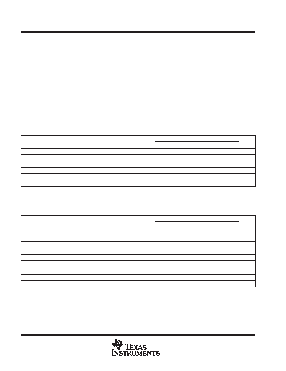
recommended operating conditions (see Note 3)
SN5400
SN7400
UNIT
MIN
NOM
MAX
MIN
NOM
MAX
UNIT
VCC
Supply voltage
4.5
5
5.5
4.75
5
5.25
V
VIH
High-level input voltage
2
V
VIL
Low-level input voltage
0.8
V
IOH
High-level output current
0.4
mA
IOL
Low-level output current
16
mA
TA
Operating free-air temperature
55
125
0
70
°C
NOTE 3: All unused inputs of the device must be held at VCC or GND to ensure proper device operation. Refer to the TI application report,
Implications of Slow or Floating CMOS Inputs, literature number SCBA004.
electrical characteristics over recommended operating free-air temperature range (unless
otherwise noted)
PARAMETER
TEST CONDITIONS
SN5400
SN7400
UNIT
PARAMETER
TEST CONDITIONS
MIN
TYP§
MAX
MIN
TYP§
MAX
UNIT
VIK
VCC = MIN,
II = 12 mA
1.5
V
VOH
VCC = MIN,
VIL = 0.8 V,
IOH = 0.4 mA
2.4
3.4
2.4
3.4
V
VOL
VCC = MIN,
VIH = 2 V,
IOL = 16 mA
0.2
0.4
0.2
0.4
V
II
VCC = MAX,
VI = 5.5 V
1
mA
IIH
VCC = MAX,
VI = 2.4 V
40
A
IIL
VCC = MAX,
VI = 0.4 V
1.6
mA
IOS
VCC = MAX
20
55
18
55
mA
ICCH
VCC = MAX,
VI = 0 V
4
8
4
8
mA
ICCL
VCC = MAX,
VI = 4.5 V
12
22
12
22
mA
For conditions shown as MIN or MAX, use the appropriate value specified under recommended operating conditions.
§ All typical values are at VCC = 5 V, TA = 25°C.
Not more than one output should be shorted at a time.
相關(guān)PDF資料 |
PDF描述 |
|---|---|
| SN74LS00PSRE4 | LS SERIES, QUAD 2-INPUT NAND GATE, PDSO8 |
| SN74LS00DE4 | LS SERIES, QUAD 2-INPUT NAND GATE, PDSO14 |
| SN7406NP3 | 7406 SERIES, HEX 1-INPUT INVERT GATE, PDIP14 |
| SNJ5416W | TTL/H/L SERIES, HEX 1-INPUT INVERT GATE, CDFP14 |
| SN7416NSRG4 | 7416 SERIES, HEX 1-INPUT INVERT GATE, PDSO14 |
相關(guān)代理商/技術(shù)參數(shù) |
參數(shù)描述 |
|---|---|
| SN7400DRE4 | 功能描述:邏輯門 Quad 2-input Positive-NAND gates RoHS:否 制造商:Texas Instruments 產(chǎn)品:OR 邏輯系列:LVC 柵極數(shù)量:2 線路數(shù)量(輸入/輸出):2 / 1 高電平輸出電流:- 16 mA 低電平輸出電流:16 mA 傳播延遲時(shí)間:3.8 ns 電源電壓-最大:5.5 V 電源電壓-最小:1.65 V 最大工作溫度:+ 125 C 安裝風(fēng)格:SMD/SMT 封裝 / 箱體:DCU-8 封裝:Reel |
| SN7400DRG4 | 功能描述:邏輯門 Quad 2-input Pos- NAND RoHS:否 制造商:Texas Instruments 產(chǎn)品:OR 邏輯系列:LVC 柵極數(shù)量:2 線路數(shù)量(輸入/輸出):2 / 1 高電平輸出電流:- 16 mA 低電平輸出電流:16 mA 傳播延遲時(shí)間:3.8 ns 電源電壓-最大:5.5 V 電源電壓-最小:1.65 V 最大工作溫度:+ 125 C 安裝風(fēng)格:SMD/SMT 封裝 / 箱體:DCU-8 封裝:Reel |
| SN7400N | 功能描述:邏輯門 Quad 2-Input RoHS:否 制造商:Texas Instruments 產(chǎn)品:OR 邏輯系列:LVC 柵極數(shù)量:2 線路數(shù)量(輸入/輸出):2 / 1 高電平輸出電流:- 16 mA 低電平輸出電流:16 mA 傳播延遲時(shí)間:3.8 ns 電源電壓-最大:5.5 V 電源電壓-最小:1.65 V 最大工作溫度:+ 125 C 安裝風(fēng)格:SMD/SMT 封裝 / 箱體:DCU-8 封裝:Reel |
| SN7400N | 制造商:Texas Instruments 功能描述:Quadruple 2 input positive NAND gate lo |
| SN7400N | 制造商:Texas Instruments 功能描述:IC 74TTL 7400 DIP14 5V |
發(fā)布緊急采購(gòu),3分鐘左右您將得到回復(fù)。