- 您現(xiàn)在的位置:買賣IC網(wǎng) > PDF目錄376410 > SN74LS195D (Motorola, Inc.) UNIVERSAL 4-BIT SHIFT REGISTER PDF資料下載
參數(shù)資料
| 型號: | SN74LS195D |
| 廠商: | Motorola, Inc. |
| 英文描述: | UNIVERSAL 4-BIT SHIFT REGISTER |
| 中文描述: | 通用4位移位寄存器 |
| 文件頁數(shù): | 2/6頁 |
| 文件大小: | 220K |
| 代理商: | SN74LS195D |

5-367
FAST AND LS TTL DATA
SN54/74LS195A
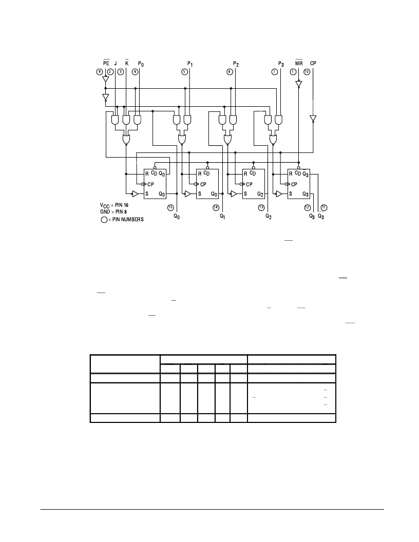
LOGIC DIAGRAM
FUNCTIONAL DESCRIPTION
The Logic Diagram and Truth Table indicate the functional
characteristics of the LS195A 4-Bit Shift Register. The device
is useful in a wide variety of shifting, counting and storage
applications. It performs serial, parallel, serial to parallel, or
parallel to serial data transfers at very high speeds.
The LS195A has two primary modes of operation, shift right
(Q0
o
Q1) and parallel load which are controlled by the state of
the Parallel Enable (PE) input. When the PE input is HIGH,
serial data enters the first flip-flop Q0 via the J and K inputs and
is shifted one bit in the direction Q0
o
Q1
o
Q2
o
Q3 following
each LOW to HIGH clock transition. The JK inputs provide the
flexibility of the JK type input for special applications, and the
simple D type input for general applications by tying the two
pins together. When the PE input is LOW, the LS195A appears
as four common clocked D flip-flops. The data on the parallel
inputs P0, P1, P2, P3 is transferred to the respective Q0, Q1,
Q2, Q3 outputs following the LOW to HIGH clock transition.
Shift left operations (Q3
o
Q2) can be achieved by tying the Qn
Outputs to the Pn–1 inputs and holding the PE input LOW.
All serial and parallel data transfers are synchronous,
occurring after each LOW to HIGH clock transition. Since the
LS195A utilizes edge-triggering, there is no restriction on the
activity of the J, K, Pn and PE inputs for logic operation —
except for the set-up and release time requirements.
A LOW on the asynchronous Master Reset (MR) input sets
all Q outputs LOW, independent of any other input condition.
MODE SELECT — TRUTH TABLE
OPERATING MODES
INPUTS
OUTPUTS
Q2
L
MR
PE
J
K
Pn
X
Q0
L
Q1
L
Q3
L
Q3
H
Asynchronous Reset
L
X
X
X
Shift, Set First Stage
Shift, Reset First
Shift, Toggle First Stage
Shift, Retain First Stage
H
H
H
H
h
h
h
h
h
I
h
I
h
I
I
h
X
X
X
X
H
L
q0
q0
p0
q0
q0
q0
q0
p1
q1
q1
q1
q1
p2
q2
q2
q2
q2
p3
q2
q2
q2
q2
p3
Parallel Load
L = LOW voltage levels
H = HIGH voltage levels
X = Don’t Care
I = LOW voltage level one set-up time prior to the LOW to HIGH clock transition.
h = HIGH voltage level one set-up time prior to the LOW to HIGH clock transition.
pn (qn) = Lower case letters indicate the state of the referenced input (or output) one set-up time prior to the LOW to
HIGH clock transition.
H
I
X
X
pn
相關PDF資料 |
PDF描述 |
|---|---|
| SN74LS195N | UNIVERSAL 4-BIT SHIFT REGISTER |
| SN54LS197J | 4-STAGE PRESETTABLE RIPPLE COUNTERS |
| SN74LS196D | 4-STAGE PRESETTABLE RIPPLE COUNTERS |
| SN74LS196N | Demonstration Circuit Board for AMMP-6530 (Mixer) |
| SN74LS197D | Demonstration Circuit Board |
相關代理商/技術參數(shù) |
參數(shù)描述 |
|---|---|
| SN74LS196D | 制造商:Rochester Electronics LLC 功能描述:- Bulk |
| SN74LS196FN | 制造商:. 功能描述: |
| SN74LS196N | 制造商:ON Semiconductor 功能描述: |
| SN74LS197N | 制造商:Texas Instruments 功能描述: |
| SN74LS19AD | 功能描述:變換器 Hex Schmitt-Trigger 變換器 RoHS:否 制造商:NXP Semiconductors 電路數(shù)量:6 邏輯系列:74ABT 邏輯類型:BiCMOS 高電平輸出電流:- 15 mA 低電平輸出電流:20 mA 傳播延遲時間:2.2 ns 電源電壓-最大:5.5 V 電源電壓-最小:4.5 V 最大工作溫度:+ 85 C 最小工作溫度:- 40 C 工作溫度范圍: 封裝 / 箱體:DIP-14 封裝:Tube |
發(fā)布緊急采購,3分鐘左右您將得到回復。