- 您現(xiàn)在的位置:買賣IC網(wǎng) > PDF目錄376417 > SN74LS95D (Motorola, Inc.) Silicon Controlled Rectifier; Package: TO-220 3 LEAD STANDARD; No of Pins: 3; Container: Rail; Qty per Container: 50 PDF資料下載
參數(shù)資料
| 型號: | SN74LS95D |
| 廠商: | Motorola, Inc. |
| 英文描述: | Silicon Controlled Rectifier; Package: TO-220 3 LEAD STANDARD; No of Pins: 3; Container: Rail; Qty per Container: 50 |
| 中文描述: | 4位移位寄存器 |
| 文件頁數(shù): | 2/6頁 |
| 文件大小: | 200K |
| 代理商: | SN74LS95D |

5-172
FAST AND LS TTL DATA
SN54/74LS95B
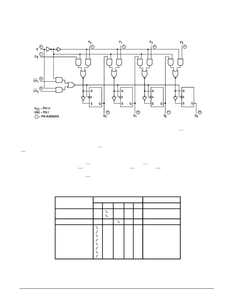
LOGIC DIAGRAM
FUNCTIONAL DESCRIPTION
The LS95B is a 4-Bit Shift Register with serial and parallel
synchronous operating modes. It has a Serial (DS) and four
Parallel (P0–P3) Data inputs and four Parallel Data outputs
(Q0–Q3). The serial or parallel mode of operation is controlled
by a Mode Control input (S) and two Clock Inputs (CP1) and
(CP2). The serial (right-shift) or parallel data transfers occur
synchronous with the HIGH to LOW transition of the selected
clock input.
When the Mode Control input (S) is HIGH, CP2 is enabled. A
HIGH to LOW transition on enabled CP2 transfers parallel
data from the P0–P3 inputs to the Q0–Q3 outputs.
When the Mode Control input (S) is LOW, CP1 is enabled. A
HIGH to LOW transition on enabled CP1 transfers the data
from Serial input (DS) to Q0 and shifts the data in Q0 to Q1, Q1
to Q2, and Q2 to Q3 respectively (right-shift). A left-shift is ac-
complished by externally connecting Q3 to P2, Q2 to P1, and
Q1 to P0, and operating the LS95B in the parallel mode (S =
HIGH).
For normal operation, S should only change states when
both Clock inputs are LOW. However, changing S from LOW
to HIGH while CP2 is HIGH, or changing S from HIGH to LOW
while CP1 is HIGH and CP2 is LOW will not cause any changes
on the register outputs.
MODE SELECT — TRUTH TABLE
OPERATING MODE
INPUTS
OUTPUTS
S
CP1
CP2
X
X
DS
I
h
Pn
X
X
Q0
L
H
Q1
q0
q0
P1
No Change
No Change
No Change
Undetermined
Undetermined
No Change
Undetermined
No Change
Q2
q1
q1
P2
Q3
q2
q2
P3
Shift
L
L
Parallel Load
H
X
X
Pn
X
X
X
X
X
X
X
X
P0
L
L
H
H
L
L
H
H
L
L
L
L
H
H
H
H
X
X
X
X
X
X
X
X
Mode Change
L = LOW Voltage Level
H = HIGH Voltage Level
X = Don’t Care
I = LOW Voltage Level one set-up time prior to the HIGH to LOW clock transition.
h = HIGH Voltage Level one set-up time prior to the HIGH to LOW clock transition.
Pn = Lower case letters indicate the state of the referenced input (or output) one set-up time prior to the
Pn
=
HIGH to LOW clock transition.
相關(guān)PDF資料 |
PDF描述 |
|---|---|
| SN74LS95B | 4-BIT SHIFT REGISTER |
| SN54LS95J | Single 2 Input AND Gate; Package: TSOP-5 / SOT23-5; No of Pins: 5; Container: Tape and Reel; Qty per Container: 3000 |
| SN74LS95N | Silicon Controlled Rectifier; Package: TO-220 3 LEAD STANDARD; No of Pins: 3; Container: Rail; Qty per Container: 50 |
| SN74LVC1GU04YZTR | SINGLE INVERTER GATE |
| SN74LVCH16240 | 16-BIT BUFFER/DRIVER WITH 3-STATE OUTPUTS |
相關(guān)代理商/技術(shù)參數(shù) |
參數(shù)描述 |
|---|---|
| SN74LS96D | 制造商:Rochester Electronics LLC 功能描述:- Bulk 制造商:Texas Instruments 功能描述: |
| SN74LV00AD | 功能描述:邏輯門 Quad 2-In Pos NAND RoHS:否 制造商:Texas Instruments 產(chǎn)品:OR 邏輯系列:LVC 柵極數(shù)量:2 線路數(shù)量(輸入/輸出):2 / 1 高電平輸出電流:- 16 mA 低電平輸出電流:16 mA 傳播延遲時間:3.8 ns 電源電壓-最大:5.5 V 電源電壓-最小:1.65 V 最大工作溫度:+ 125 C 安裝風(fēng)格:SMD/SMT 封裝 / 箱體:DCU-8 封裝:Reel |
| SN74LV00AD | 制造商:Texas Instruments 功能描述:GATE / INVERTER LOGIC IC |
| SN74LV00ADBR | 功能描述:邏輯門 Quad 2-In Pos NAND RoHS:否 制造商:Texas Instruments 產(chǎn)品:OR 邏輯系列:LVC 柵極數(shù)量:2 線路數(shù)量(輸入/輸出):2 / 1 高電平輸出電流:- 16 mA 低電平輸出電流:16 mA 傳播延遲時間:3.8 ns 電源電壓-最大:5.5 V 電源電壓-最小:1.65 V 最大工作溫度:+ 125 C 安裝風(fēng)格:SMD/SMT 封裝 / 箱體:DCU-8 封裝:Reel |
| SN74LV00ADBRG4 | 功能描述:邏輯門 Quadruple 2-Input Positive-NAND gates RoHS:否 制造商:Texas Instruments 產(chǎn)品:OR 邏輯系列:LVC 柵極數(shù)量:2 線路數(shù)量(輸入/輸出):2 / 1 高電平輸出電流:- 16 mA 低電平輸出電流:16 mA 傳播延遲時間:3.8 ns 電源電壓-最大:5.5 V 電源電壓-最小:1.65 V 最大工作溫度:+ 125 C 安裝風(fēng)格:SMD/SMT 封裝 / 箱體:DCU-8 封裝:Reel |
發(fā)布緊急采購,3分鐘左右您將得到回復(fù)。