- 您現(xiàn)在的位置:買賣IC網(wǎng) > PDF目錄376417 > SNJ54ACT1284J (Texas Instruments, Inc.) 7-BIT BUS INTERFACES WITH 3-STATE OUTPUTS PDF資料下載
參數(shù)資料
| 型號: | SNJ54ACT1284J |
| 廠商: | Texas Instruments, Inc. |
| 英文描述: | 7-BIT BUS INTERFACES WITH 3-STATE OUTPUTS |
| 中文描述: | 7位總線接口與三態(tài)輸出 |
| 文件頁數(shù): | 1/12頁 |
| 文件大小: | 291K |
| 代理商: | SNJ54ACT1284J |

SCAS459D NOVEMBER 1994 REVISED OCTOBER 2003
1
POST OFFICE BOX 655303
DALLAS, TEXAS 75265
4.5-V to 5.5-V V
CC
Operation
Inputs Accept Voltages to 5.5 V
Max t
pd
of 20 ns at 5 V
3-State Outputs Directly Drive Bus Lines
Flow-Through Architecture Optimizes PCB
Layout
Center-Pin V
CC
and GND Configurations
Minimize High-Speed Switching Noise
ESD Protection Exceeds JESD 22
2000-V Human-Body Model (A114-A)
200-V Machine Model (A115-A)
Designed for the IEEE 1284-I (Level-1 Type)
and IEEE 1284-II (Level-2 Type) Electrical
Specifications
description/ordering information
The ’ACT1284 devices are designed for
asynchronous two-way communication between
data buses. The control function minimizes
external timing requirements.
The devices allow data transmission in either the
A-to-B or the B-to-A direction for bits 1, 2, 3, and
4, depending on the logic level at the
direction-control (DIR) input. Bits 5, 6, and 7,
however, always transmit in the A-to-B direction.
The output drive for each mode is determined by the high-drive (HD) control pin. When HD is high, the high drive
is delivered by the totem-pole configuration, and when HD is low, the outputs are open drain. This meets the
drive requirements as specified in the IEEE 1284-I (level-1 type) and the IEEE 1284-II (level-2 type) parallel
peripheral-interface specification.
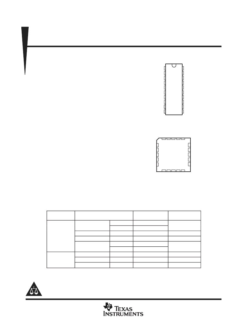
ORDERING INFORMATION
TA
PACKAGE
ORDERABLE
PART NUMBER
TOP-SIDE
MARKING
SOIC DW
Tube
SN74ACT1284DW
ACT1284
Tape and reel
SN74ACT1284DWR
0
°
C to 70
°
C
SOP NS
Tape and reel
SN74ACT1284NSR
ACT1284
SSOP DB
Tape and reel
SN74ACT1284DBR
AU284
TSSOP PW
Tube
SN74ACT1284PW
AU284
Tape and reel
SN74ACT1284PWR
CDIP J
Tube
SNJ54ACT1284J
SNJ54ACT1284J
55 C to 125 C
CFP W
Tube
SNJ54ACT1284W
SNJ54ACT1284W
LCCC FK
Tube
SNJ54ACT1284FK
SNJ54ACT1284FK
Package drawings, standard packing quantities, thermal data, symbolization, and PCB design guidelines are
available at www.ti.com/sc/package.
Copyright
2003, Texas Instruments Incorporated
!"#$%& "!&'&
&(!)$'!& "#))%& ' !( *#+,"'!& '%- )!#"
*%"("'!&
*%) % %)$ !( %.'
)!#"!&
*)!"%&1
!%
*')'$%%)-
"!&(!)$ !
/'))'&0-
&)#$%&
'&')
&! &%"%'),0
&",#% %&1
!( ',,
Please be aware that an important notice concerning availability, standard warranty, and use in critical applications of
Texas Instruments semiconductor products and disclaimers thereto appears at the end of this data sheet.
1
2
3
4
5
6
7
8
9
10
20
19
18
17
16
15
14
13
12
11
A1
A2
A3
A4
GND
GND
A5
A6
A7
DIR
B1
B2
B3
B4
V
CC
V
CC
B5
B6
B7
HD
SN54ACT1284 . . . J OR W PACKAGE
SN74ACT1284 . . . DB, DW, NS, OR PW PACKAGE
(TOP VIEW)
3
2
1 20 19
9 10 11 12 13
4
5
6
7
8
18
17
16
15
14
B3
B4
V
CC
V
CC
B5
A4
GND
GND
A5
A6
SN54ACT1284 . . . FK PACKAGE
(TOP VIEW)
A
A
A
B
B
B
A
D
H
B
相關(guān)PDF資料 |
PDF描述 |
|---|---|
| SNJ54ACT1284W | 7-BIT BUS INTERFACES WITH 3-STATE OUTPUTS |
| SNJ54ACT245K | OCTAL BUS TRANSCEIVERS WITH 3-STATE OUTPUTS |
| SNJ54AHC05FK | HEX INVERTERS WITH OPEN-DRAIN OUTPUTS |
| SNJ54AHC05J | HEX INVERTERS WITH OPEN-DRAIN OUTPUTS |
| SNJ54AHC05W | HEX INVERTERS WITH OPEN-DRAIN OUTPUTS |
相關(guān)代理商/技術(shù)參數(shù) |
參數(shù)描述 |
|---|---|
| SNJ54ACT1284W | 制造商:TI 制造商全稱:Texas Instruments 功能描述:7-BIT BUS INTERFACES WITH 3-STATE OUTPUTS |
| SNJ54ACT14FK | 制造商:Texas Instruments 功能描述:Inverter Schmitt Trigger 6-Element CMOS 20-Pin LCCC Tube |
| SNJ54ACT14J | 制造商:Texas Instruments 功能描述:5962-9218301MCA HEX SCHMITT-TRIG INVERT 制造商:Texas Instruments 功能描述:5962-9218301MCA, HEX SCHMITT-TRIG INVERT - Rail/Tube 制造商:Texas Instruments 功能描述:Inverter Schmitt Trigger 6-Element CMOS 14-Pin CDIP Tube |
| SNJ54ACT14W | 制造商:Texas Instruments 功能描述: |
| SNJ54ACT16244WD | 制造商:Texas Instruments 功能描述: 制造商:Texas Instruments 功能描述:16-BIT BUFFERS/LIN DRIVERS |
發(fā)布緊急采購,3分鐘左右您將得到回復。