- 您現(xiàn)在的位置:買賣IC網(wǎng) > PDF目錄373479 > SNJ54LV240AW (Texas Instruments, Inc.) OCTAL BUFFERS/DRIVERS WITH 3-STATE OUTPUTS PDF資料下載
參數(shù)資料
| 型號: | SNJ54LV240AW |
| 廠商: | Texas Instruments, Inc. |
| 英文描述: | OCTAL BUFFERS/DRIVERS WITH 3-STATE OUTPUTS |
| 中文描述: | 八路緩沖器/ 3司機態(tài)輸出 |
| 文件頁數(shù): | 1/15頁 |
| 文件大?。?/td> | 357K |
| 代理商: | SNJ54LV240AW |
SCLS384H SEPTEMBER 1997 REVISED APRIL 2005
1
POST OFFICE BOX 655303
DALLAS, TEXAS 75265
2-V to 5.5-V V
CC
Operation
Max t
pd
of 6.5 ns at 5 V
Typical V
OLP
(Output Ground Bounce)
<0.8 V at V
CC
= 3.3 V, T
A
= 25
°
C
Typical V
OHV
(Output V
OH
Undershoot)
>2.3 V at V
CC
= 3.3 V, T
A
= 25
°
C
Support Mixed-Mode Voltage Operation on
All Ports
Latch-Up Performance Exceeds 250 mA Per
JESD 17
ESD Protection Exceeds JESD 22
2000-V Human-Body Model (A114-A)
200-V Machine Model (A115-A)
1000-V Charged-Device Model (C101)
description/ordering information
These octal buffers/drivers are designed for 2-V to
5.5-V V
CC
operation.
The ’LV240A devices are designed specifically to
improve both the performance and density of
3-state memory address drivers, clock drivers,
and bus-oriented receivers and transmitters.
These devices are organized as two 4-bit
buffers/line drivers with separate output-enable
(OE) inputs. When OE is low, the device passes
data from the A inputs to the Y outputs. When OE
is high, the outputs are in the high-impedance
state.
ORDERING INFORMATION
TA
PACKAGE
ORDERABLE
PART NUMBER
TOP-SIDE
MARKING
SOIC DW
Tube of 25
SN74LV240ADW
LV240A
Reel of 2000
SN74LV240ADWR
SOP NS
Reel of 2000
SN74LV240ANSR
74LV240A
40
°
C to 85
°
C
SSOP DB
Reel of 2000
SN74LV240ADBR
LV240A
Tube of 70
SN74LV240APW
TSSOP PW
Reel of 2000
SN74LV240APWR
LV240A
Reel of 250
SN74LV240APWT
TVSOP DGV
Reel of 2000
SN74LV240ADGVR
LV240A
CDIP J
Tube of 20
SNJ54LV240AJ
SNJ54LV240AJ
55 C to 125 C
CFP W
LCCC FK
Tube of 85
Tube of 55
SNJ54LV240AW
SNJ54LV240AFK
SNJ54LV240AW
SNJ54LV240AFK
Package drawings, standard packing quantities, thermal data, symbolization, and PCB design
guidelines are available at www.ti.com/sc/package.
Copyright
2005, Texas Instruments Incorporated
!"#$%&' #"'('
')"*%("' #$**&' ( ") +$,-#("' !(&. *"!$#
+&#)#("'
+&* & &*% ") &/(
*"!$#"'
+*"#&'2
!"& '" '&#&(*-1
+(*(%&&*.
#"')"*% "
'*$%&'
('!(*! 0(**('1.
'#-$!& &'2
") (--
Please be aware that an important notice concerning availability, standard warranty, and use in critical applications of
Texas Instruments semiconductor products and disclaimers thereto appears at the end of this data sheet.
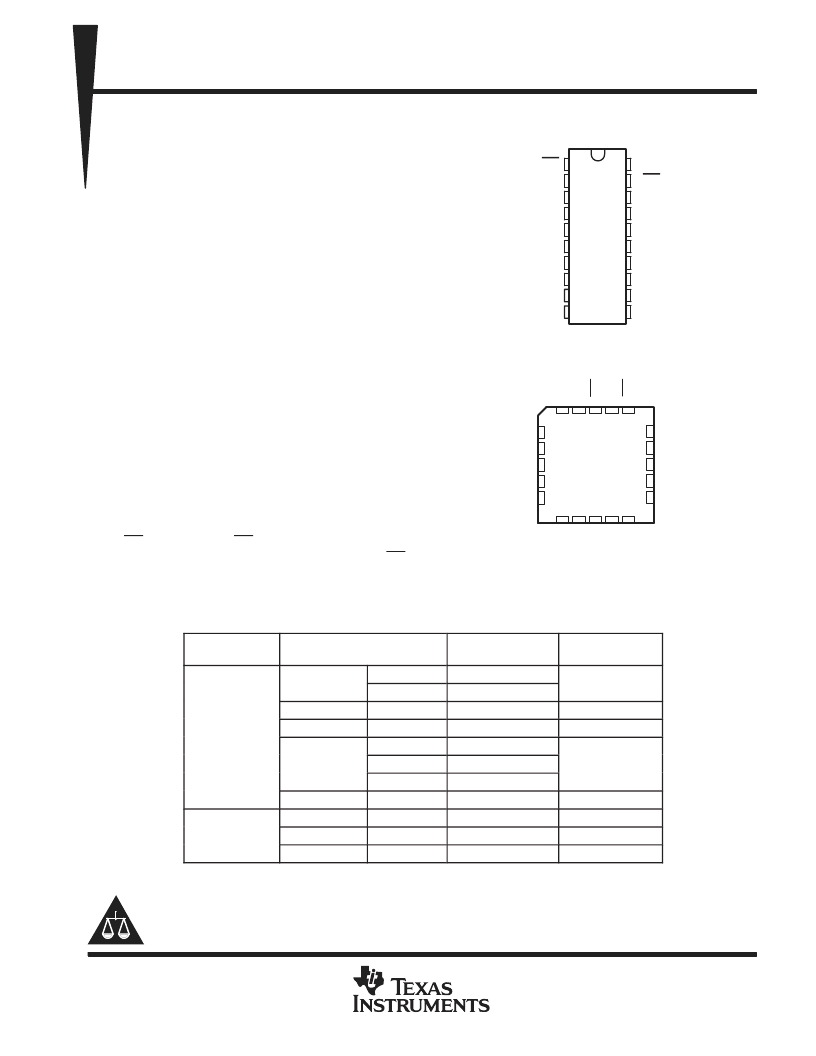
1
2
3
4
5
6
7
8
9
10
20
19
18
17
16
15
14
13
12
11
1OE
1A1
2Y4
1A2
2Y3
1A3
2Y2
1A4
2Y1
GND
V
CC
2OE
1Y1
2A4
1Y2
2A3
1Y3
2A2
1Y4
2A1
SN54LV240A . . . J OR W PACKAGE
SN74LV240A . . . DB, DGV, DW, NS, OR PW PACKAGE
(TOP VIEW)
3
2
1 20 19
9 10 11 12 13
4
5
6
7
8
18
17
16
15
14
1Y1
2A4
1Y2
2A3
1Y3
1A2
2Y3
1A3
2Y2
1A4
SN54LV240A . . . FK PACKAGE
(TOP VIEW)
2
1
1
1
2
2
2
G
2
V
C
相關(guān)PDF資料 |
PDF描述 |
|---|---|
| SN74LV245ATGVR | OCTAL BUS TRANSCEIVER WITH 3-STATE OUTPUTS |
| SN74LV374ARGYRG4 | OCTAL EDGE-TRIGGERED D-TYPE FLIP-FLOPS WITH 3-STATE OUTPUTS |
| SN74LV393ADB | DUAL 4-BIT BINARY COUNTERS |
| SN74LV4040ADB | Bipolar Power DPAK PNP 6A 100V; Package: DPAK-3 (SINGLE GAUGE); No of Pins: 4; Container: Rail; Qty per Container: 75 |
| SN54LV4040A | Octal D-Type Flip-Flop; Package: TSSOP 20 LEAD; No of Pins: 20; Container: Tape and Reel; Qty per Container: 2500 |
相關(guān)代理商/技術(shù)參數(shù) |
參數(shù)描述 |
|---|---|
| SNJ54LVC00AFK | 制造商:Texas Instruments 功能描述: 制造商:Texas Instruments 功能描述:QUADRUPLE 2-INPUT POSITIVE-NAND GATE |
| SNJ54LVC00AJ | 制造商:Texas Instruments 功能描述:5962-9753301QCA, QUAD 2-IN POS-NAND GATE - Rail/Tube |
| SNJ54LVC00AW | 制造商:Texas Instruments 功能描述: |
| SNJ54LVC02AFK | 制造商:Texas Instruments 功能描述: |
| SNJ54LVC02AW | 制造商:Texas Instruments 功能描述:NOR Gate 4-Element 2-IN CMOS 14-Pin CFPAK Tube |
發(fā)布緊急采購,3分鐘左右您將得到回復。