- 您現(xiàn)在的位置:買賣IC網(wǎng) > PDF目錄98140 > SNJ54LVT244W (TEXAS INSTRUMENTS INC) LVT SERIES, DUAL 4-BIT DRIVER, TRUE OUTPUT, CDFP20 PDF資料下載
參數(shù)資料
| 型號(hào): | SNJ54LVT244W |
| 廠商: | TEXAS INSTRUMENTS INC |
| 元件分類: | 總線收發(fā)器 |
| 英文描述: | LVT SERIES, DUAL 4-BIT DRIVER, TRUE OUTPUT, CDFP20 |
| 封裝: | CERAMIC, FP-20 |
| 文件頁(yè)數(shù): | 6/13頁(yè) |
| 文件大小: | 386K |
| 代理商: | SNJ54LVT244W |
第1頁(yè)第2頁(yè)第3頁(yè)第4頁(yè)第5頁(yè)當(dāng)前第6頁(yè)第7頁(yè)第8頁(yè)第9頁(yè)第10頁(yè)第11頁(yè)第12頁(yè)第13頁(yè)
SN54LVT244, SN74LVT244
3.3-V ABT OCTAL BUFFERS/DRIVERS
WITH 3-STATE OUTPUTS
SCBS135B – AUGUST 1992 – REVISED MARCH 1994
2–2
POST OFFICE BOX 655303
DALLAS, TEXAS 75265
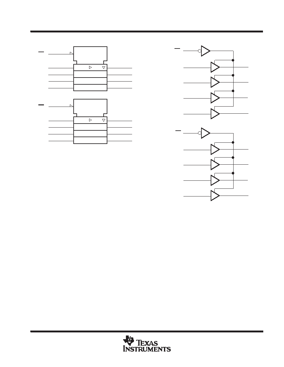
logic symbol
logic diagram (positive logic)
1
2
4
6
8
19
11
13
15
17
3
5
7
9
12
14
16
18
1A1
1A2
1A3
1A4
1Y1
2A1
2A2
2A3
2A4
2Y1
1Y2
1Y3
1Y4
2Y2
2Y3
2Y4
2OE
1OE
2
1A1
4
1A2
6
1A3
8
1A4
EN
1
1Y1
18
1Y2
16
1Y3
14
1Y4
12
11
2A1
13
2A2
15
2A3
17
2A4
EN
19
2Y1
9
2Y2
7
2Y3
5
2Y4
3
1OE
2OE
This symbol is in accordance with ANSI/IEEE Std 91-1984
and IEC Publication 617-12.
absolute maximum ratings over operating free-air temperature range (unless otherwise noted)
Supply voltage range, VCC
– 0.5 V to 4.6 V
. . . . . . . . . . . . . . . . . . . . . . . . . . . . . . . . . . . . . . . . . . . . . . . . . . . . . . . .
Input voltage range, VI (see Note 1)
– 0.5 V to 7 V
. . . . . . . . . . . . . . . . . . . . . . . . . . . . . . . . . . . . . . . . . . . . . . . . . .
Voltage range applied to any output in the high state or power-off state, VO (see Note 1)
– 0.5 V to 7 V
. . . .
Current into any output in the low state, IO: SN54LVT244
96 mA
. . . . . . . . . . . . . . . . . . . . . . . . . . . . . . . . . . . .
SN74LVT244
128 mA
. . . . . . . . . . . . . . . . . . . . . . . . . . . . . . . . . . . .
Current into any output in the high state, IO (see Note 2): SN54LVT244
48 mA
. . . . . . . . . . . . . . . . . . . . . . . . .
SN74LVT244
64 mA
. . . . . . . . . . . . . . . . . . . . . . . . .
Input clamp current, IIK (VI < 0)
– 50 mA
. . . . . . . . . . . . . . . . . . . . . . . . . . . . . . . . . . . . . . . . . . . . . . . . . . . . . . . . . .
Output clamp current, IOK (VO < 0)
– 50 mA
. . . . . . . . . . . . . . . . . . . . . . . . . . . . . . . . . . . . . . . . . . . . . . . . . . . . . . .
Maximum power dissipation at TA = 55°C (in still air) (see Note 3): DB package
0.6 W
. . . . . . . . . . . . . . . . . . . .
DW package
1.6 W
. . . . . . . . . . . . . . . . . . .
PW package
0.7 W
. . . . . . . . . . . . . . . . . . .
Storage temperature range
– 65
°C to 150°C
. . . . . . . . . . . . . . . . . . . . . . . . . . . . . . . . . . . . . . . . . . . . . . . . . . . . . . .
Stresses beyond those listed under “absolute maximum ratings” may cause permanent damage to the device. These are stress ratings only and
functional operation of the device at these or any other conditions beyond those indicated under “recommended operating conditions” is not
implied. Exposure to absolute-maximum-rated conditions for extended periods may affect device reliability.
NOTES:
1. The input and output negative-voltage ratings may be exceeded if the input and output clamp-current ratings are observed.
2. This current will only flow when the output is in the high state and VO > VCC.
3. The maximum package power dissipation is calculated using a junction temperature of 150
°C and a board trace length of 750 mils.
For more information, refer to the
Package Thermal Considerations application note.
LVT244–5
相關(guān)PDF資料 |
PDF描述 |
|---|---|
| SNJ54LVTH125FK | LVT SERIES, QUAD 1-BIT DRIVER, TRUE OUTPUT, CQCC20 |
| SNJ54LVTH16646WD | LVT SERIES, DUAL 8-BIT REGISTERED TRANSCEIVER, TRUE OUTPUT, CDFP56 |
| SNJ54LVTH182245WD | LVT SERIES, DUAL 9-BIT BOUNDARY SCAN TRANSCEIVER, TRUE OUTPUT, CDFP56 |
| SN74LVTH182245DGGR | LVT SERIES, DUAL 9-BIT BOUNDARY SCAN TRANSCEIVER, TRUE OUTPUT, PDSO56 |
| SNJ54LVTH182514HKC | LVT SERIES, 20-BIT BOUNDARY SCAN REG TRANSCEIVER, TRUE OUTPUT, CDFP64 |
相關(guān)代理商/技術(shù)參數(shù) |
參數(shù)描述 |
|---|---|
| SNJ54LVT245FK | 制造商:Rochester Electronics LLC 功能描述:- Bulk 制造商:Texas Instruments 功能描述: |
| SNJ54LVT245J | 制造商:Texas Instruments 功能描述: |
| SNJ54LVT573FK | 制造商:Rochester Electronics LLC 功能描述:- Bulk 制造商:Texas Instruments 功能描述: |
| SNJ54LVT574FK | 制造商:Rochester Electronics LLC 功能描述:OCTAL BUS DRIVER, DSCC 5962-9583201Q2A - Bulk 制造商:Texas Instruments 功能描述: |
| SNJ54LVT574W | 制造商:Texas Instruments 功能描述: |
發(fā)布緊急采購(gòu),3分鐘左右您將得到回復(fù)。