- 您現(xiàn)在的位置:買賣IC網(wǎng) > PDF目錄372173 > SP319 5V High-Speed RS-232 Transceivers with 0.1uF Capacitors PDF資料下載
參數(shù)資料
| 型號(hào): | SP319 |
| 元件分類: | RS-232 |
| 英文描述: | 5V High-Speed RS-232 Transceivers with 0.1uF Capacitors |
| 中文描述: | 5V的高速RS - 232收發(fā)器與0.1uF電容 |
| 文件頁(yè)數(shù): | 2/14頁(yè) |
| 文件大?。?/td> | 222K |
| 代理商: | SP319 |
第1頁(yè)當(dāng)前第2頁(yè)第3頁(yè)第4頁(yè)第5頁(yè)第6頁(yè)第7頁(yè)第8頁(yè)第9頁(yè)第10頁(yè)第11頁(yè)第12頁(yè)第13頁(yè)第14頁(yè)
2
SP319DS/08 SP319 20Mbps, +5V-Only V.35 Interface with RS-232 (V.28) Control Lines Copyright 2000 Sipex Corporation
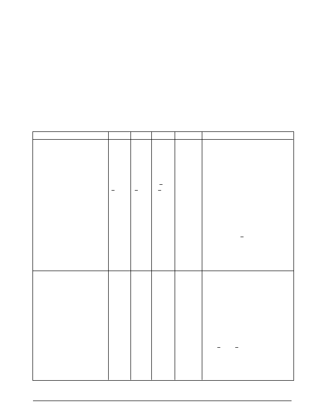
ABSOLUTE MAXIMUM RATINGS
These are stress ratings only and functional operation of the device at
these ratings or any other above those indicated in the operation
sections of the specifications below is not implied. Exposure to absolute
maximum rating conditions for extended periods of time may affect
reliability.
V
.....................................................................................................+7V
Input Voltages
Logic........................................................-0.3V to (V
CC
+0.5V)
Drivers..................................................-0.3V to (V
CC
+0.5V)
Receivers..................................................
±
30V at
≤
100mA
Output Voltages
Logic........................................................-0.3V to (V
+0.5V)
Drivers.......................................................................
±
14V
Receivers..............................................-0.3V to (V
+0.5V)
Storage Temperature.......................................................-65C to +150C
Power Dissipation per Package
80-pin QFP (derate 18.3mW/
o
C above +70
o
C)..........................1500mW
SPECIFICATIONS
T
AMB
= T
MIN
to T
MAX
and V
CC
= 5V
±
5% unless otherwise noted.
PARAMETER
MIN.
TYP.
MAX.
UNITS
CONDITIONS
V.35 DRIVER
TTL Input Levels
V
IL
V
IH
0.8
Volts
Volts
2.0
Voltage Outputs
Open Circuit Voltage
Differential Outputs
Source Impedance
Short Circuit Impedance
+1.2
+0.66
150
165
Volts
Volts
Ohms
Ohms
Refer to Figure 1
R
=100
from A to B; Figure 2
Figure 4
Measured from A=B to Gnd,
V
OUT
=-2V to +2V; Figure 5 T
= +25
o
C
V
Offset
={[|V
A
|+|V
B
|]/2}; Figure 3
+0.44
50
135
+0.55
100
150
Voltage Output Offset
-0.6
+0.6
Volts
AC Characteristics
Transition Time
Maximum Transmission Rate
Propagation Delay
t
PHL
T
= +25
o
C for all AC parameters
10% to 90%; Figure 6
V
DIFF OUT
= 0.55V+20% ; Figure 9
40
ns
Mbps
10
80
100
ns
Measured from 1.5V of V
to 50% of V
; Figure 9 10
Measured from 1.5V of V
to 50% of V
OUT
; Figure 9 10
t
PLH
80
100
ns
V.35 RECEIVER
TTL Output Levels
V
OL
V
Receiver Inputs
Differential Input
Threshold
Input Impedance
Short Circuit Impedance
0.4
Volts
Volts
I
OUT
=-3.2mA
I
OUT
=1.0mA
2.4
-0.3
90
135
+0.3
110
165
Volts
Ohms
Ohms
100
150
Figure 7
Measured from A=B to Gnd
V
IN
=-2V to +2V; Figure 8 T
AMB
= +25
o
C
AC Characteristics
Maximum Transmission Rate
Propagation Delay
t
PHL
T
AMB
= +25
o
C for all AC parameters
V
IN
= +0.55V +20%; Figure 9
10
Mbps
60
80
ns
Measured from 50% of V
IN
to
1.5V of R
; Figure 9, 11
Measured from 50% of V
IN
to
1.5V of R
OUT
; Figure 9, 11
t
PLH
60
80
ns
相關(guān)PDF資料 |
PDF描述 |
|---|---|
| SP319CF | 5V High-Speed RS-232 Transceivers with 0.1uF Capacitors |
| SP3203EY | 5V High-Speed RS-232 Transceivers with 0.1uF Capacitors |
| SP3203 | 5V High-Speed RS-232 Transceivers with 0.1uF Capacitors |
| SP3203CY | 5V High-Speed RS-232 Transceivers with 0.1uF Capacitors |
| SP3203E | 5V High-Speed RS-232 Transceivers with 0.1uF Capacitors |
相關(guān)代理商/技術(shù)參數(shù) |
參數(shù)描述 |
|---|---|
| SP319CF | 制造商:SIPEX 制造商全稱:Sipex Corporation 功能描述:20Mbps, 5V-Only V.35 Interface with RS-232 V.28 Control Lines |
| SP319CF-L | 制造商:Exar Corporation 功能描述:TRANSCEIVER V.35 RS-232 5V 319 |
| SP31R0JT | 功能描述:電流傳感電阻器 - SMD SP3 1R0 5% TAPED RoHS:否 制造商:Vishay/Dale 電阻:10 mOhms 功率額定值:1 W 容差:1 % 外殼代碼 - in:2512 外殼代碼 - mm:6432 溫度系數(shù):75 PPM / C 系列:WSL 工作溫度范圍:- 65 C to + 170 C 產(chǎn)品:Power Metal Strip Resistors Low Value |
| SP32 | 制造商:VOLT PLASTICS 功能描述: |
| SP-32 | 制造商:Triad Magnetics 功能描述: |
發(fā)布緊急采購(gòu),3分鐘左右您將得到回復(fù)。