- 您現(xiàn)在的位置:買賣IC網(wǎng) > PDF目錄372175 > SP3222BEP 5V High-Speed RS-232 Transceivers with 0.1uF Capacitors PDF資料下載
參數(shù)資料
| 型號: | SP3222BEP |
| 元件分類: | RS-232 |
| 英文描述: | 5V High-Speed RS-232 Transceivers with 0.1uF Capacitors |
| 中文描述: | 5V的高速RS - 232收發(fā)器與0.1uF電容 |
| 文件頁數(shù): | 11/18頁 |
| 文件大小: | 139K |
| 代理商: | SP3222BEP |

11
Rev. 6/30/03 SP3222B/3232B True +3.0 to +5.5V RS-232 Transceivers
Copyright 2003 Sipex Corporation
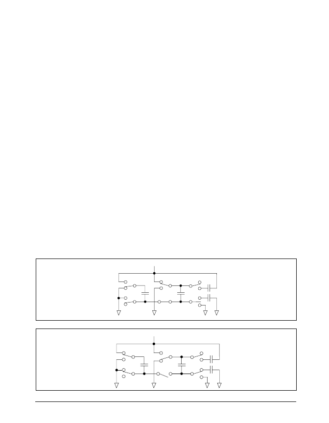
This voltage is regulated to +5.5V. At this
voltage, the internal oscillator is disabled. Si-
multaneous with the transfer of the voltage to
C
, the positive side of capacitor C
is switched
to V
and the negative side is connected to
GND, allowing the charge pump cycle to begin
again. The charge pump cycle will continue as
long as the operational conditions for the inter-
nal oscillator are present.
Since both V
+
and V
–
are separately generated
from V
; in a no–load condition V
+
and V
–
will
be symmetrical. Older charge pump approaches
that generate V
–
from V
+
will show a decrease in
the magnitude of V
–
compared to V
+
due to the
inherent inefficiencies in the design.
The clock rate for the charge pump typically
operates at 250kHz. The external capacitors can
be as low as 0.1
μ
F with a 16V breakdown
voltage rating.
ESD Tolerance
The
SP3222B/3232B
series incorporates
ruggedized ESD cells on all driver output and
receiver input pins. The ESD structure is
improved over our previous family for more
rugged applications and environments sensitive
to electrostatic discharges and associated
transients.
The Human Body Model has been the generally
accepted ESD testing method for semiconduc-
tors. This method is also specified in MIL-STD-
883, Method 3015.7 for ESD testing. The premise
of this ESD test is to simulate the human body’s
potential to store electrostatic energy and
discharge it to an integrated circuit.
The simulation is performed by using a test
model as shown in
Figure 18
. This method
will test the IC’s capability to withstand an
ESD transient during normal handling such as
in manufacturing areas where the ICs tend to
be handled frequently.
For the Human Body Model, the current
limiting resistor (R
) and the source capacitor
(C
S
) are 1.5k
and 100pF, respectively.
Figure 13. Charge Pump — Phase 1
Figure 14. Charge Pump — Phase 2
V
CC
= +5V
–5V
–5V
+5V
V
SS
Storage Capacitor
V
DD
Storage Capacitor
C
1
C
2
C
3
C
4
+
+
+
+
–
–
–
–
V
CC
= +5V
–10V
V
SS
Storage Capacitor
V
DD
Storage Capacitor
C
1
C
2
C
3
C
4
+
+
+
+
–
–
–
–
相關PDF資料 |
PDF描述 |
|---|---|
| SP3222EEP | 5V High-Speed RS-232 Transceivers with 0.1uF Capacitors |
| SP3232EEN | 5V High-Speed RS-232 Transceivers with 0.1uF Capacitors |
| SP3222ECA | 5V High-Speed RS-232 Transceivers with 0.1uF Capacitors |
| SP3222EEA | 5V High-Speed RS-232 Transceivers with 0.1uF Capacitors |
| SP3222EHCA | 5V High-Speed RS-232 Transceivers with 0.1uF Capacitors |
相關代理商/技術參數(shù) |
參數(shù)描述 |
|---|---|
| SP3222BET | 制造商:SIPEX 制造商全稱:Sipex Corporation 功能描述:True +3.0V to +5.5V RS-232 Transceivers |
| SP3222BEY | 制造商:SIPEX 制造商全稱:Sipex Corporation 功能描述:True +3.0V to +5.5V RS-232 Transceivers |
| SP3222CA | 制造商:SIPEX 制造商全稱:Sipex Corporation 功能描述:True +3.0V to +5.5V RS-232 Transceivers |
| SP3222CP | 制造商:SIPEX 制造商全稱:Sipex Corporation 功能描述:True +3.0V to +5.5V RS-232 Transceivers |
| SP3222CT | 制造商:SIPEX 制造商全稱:Sipex Corporation 功能描述:True +3.0V to +5.5V RS-232 Transceivers |
發(fā)布緊急采購,3分鐘左右您將得到回復。