- 您現(xiàn)在的位置:買賣IC網(wǎng) > PDF目錄372181 > SP385E-1ET Low Power 5V RS232 Dual Driver/Receiver with 0.1?μF Capacitors; Package: SO; No of Pins: 16; Temperature Range: -40?°C to 85?°C PDF資料下載
參數(shù)資料
| 型號: | SP385E-1ET |
| 元件分類: | 外設(shè)及接口 |
| 英文描述: | Low Power 5V RS232 Dual Driver/Receiver with 0.1?μF Capacitors; Package: SO; No of Pins: 16; Temperature Range: -40?°C to 85?°C |
| 中文描述: | 電可擦除可編程邏輯器件 |
| 文件頁數(shù): | 6/11頁 |
| 文件大小: | 98K |
| 代理商: | SP385E-1ET |

Rev. 07/26/02 SP385E-1 True +3V to +5V RS-232 Line Driver/Receiver Copyright 2002 Sipex Corporation
6
CHARGE PUMP
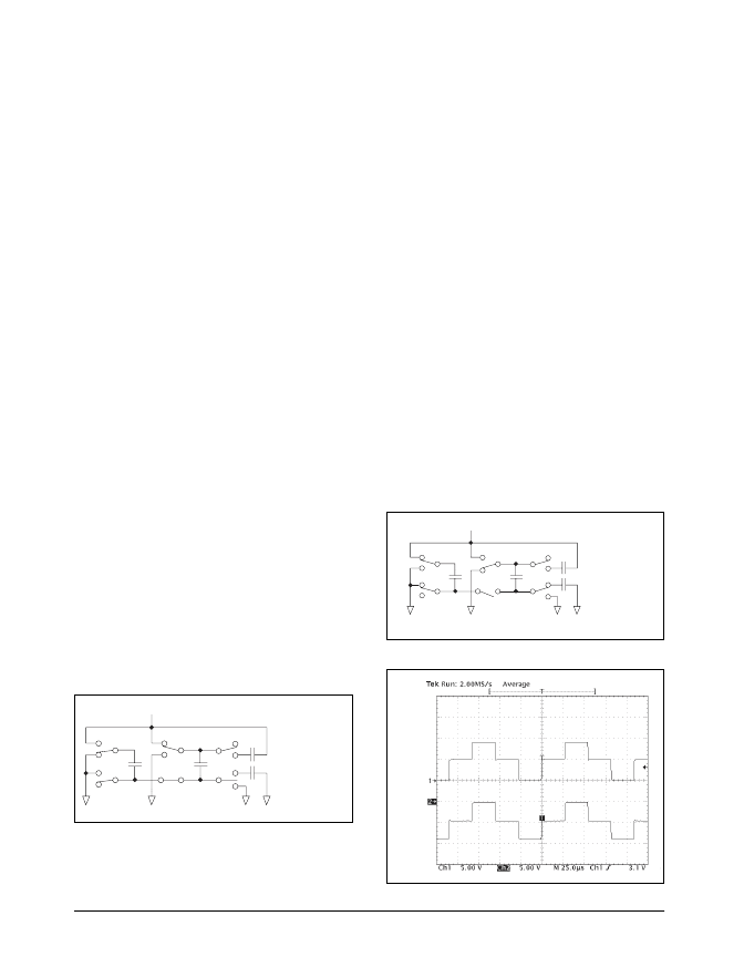
The charge pump is a
Sipex
–patented design
(5,306,954) and uses a unique approach
compared to older less–efficient designs. The
charge pump still requires four external
capacitors, but uses a four–phase voltage
shifting technique to attain symmetrical 10V
power supplies. There is a free–running
oscillator that controls the four phases of the
voltage shifting. A description of each phase
follows.
Phase 1
— V
SS
charge storage —During this phase of
the clock cycle, the positive side of capacitors
C
1
and C
2
are initially charged to +5V. C
l+
is
then switched to ground and the charge in C
1–
is transferred to C
2–
. Since C
2+
is connected to
+5V, the voltage potential across capacitor C
2
is now 10V.
Phase 2
— V
SS
transfer — Phase two of the clock
connects the negative terminal of C
2
to the
V
SS
storage capacitor and the positive
terminal of C
2
to ground, and transfers the
generated –l0V to C
3
. Simultaneously, the
positive side of capacitor C
1
is switched to
+5V and the negative side is connected to
ground.
Phase 3
— V
DD
charge storage — The third phase of
the clock is identical to the first phase — the
charge transferred in C
1
produces –5V in the
negative terminal of C
1
, which is applied to
the negative side of capacitor C
2
. Since C
2+
is
at +5V, the voltage potential across C
2
is l0V.
Phase 4
— V
DD
transfer — The fourth phase of the
clock connects the negative terminal of C
2
to
ground,
and transfers the generated l0V across C
2
to
C
4
, the V
DD
storage capacitor. Again, simulta-
neously
with this, the positive side of capacitor C
1
is
switched to +5V and the negative side is
connected to ground, and the cycle begins
again.
Since both V
+
and V
–
are separately generated
from V
CC
; in a no–load condition V
+
and V
–
will
be symmetrical. Older charge pump ap-
proaches that generate V
–
from V
+
will show
a decrease in the magnitude of V
–
compared
to V
+
due to the inherent inefficiencies in the
design.
The clock rate for the charge pump typically
operates at 15kHz. The external capacitors
can be as low as 0.1
μ
F with a 16V breakdown
voltage rating.
Figure 1. Charge Pump — Phase 1
Figure 2. Charge Pump — Phase 2
Figure 3. Charge Pump Waveforms
10V
GND
GND
-10V
V
CC
= +5V
–5V
–5V
+5V
V
SS
Storage Capacitor
V
DD
Storage Capacitor
C
1
C
2
C
3
C
4
+
+
+
+
–
–
–
–
V
CC
= +5V
–10V
V
SS
Storage Capacitor
V
DD
Storage Capacitor
C
1
C
2
C
3
C
4
+
+
+
+
–
–
–
–
C2+
C2-
相關(guān)PDF資料 |
PDF描述 |
|---|---|
| SP385E | Low Power 5V RS232 Dual Driver/Receiver with 0.1?μF Capacitors; Package: SO; No of Pins: 16; Temperature Range: -40?°C to 85?°C |
| SP385ECA | Low Power 5V RS232 Dual Driver/Receiver with 0.1?μF Capacitors; Package: SO; No of Pins: 16; Temperature Range: -40?°C to 85?°C |
| SP385ECT | Low Power 5V RS232 Dual Driver/Receiver with 0.1?μF Capacitors; Package: SO; No of Pins: 16; Temperature Range: -40?°C to 85?°C |
| SP385EET | Low Power 5V RS232 Dual Driver/Receiver with 0.1?μF Capacitors; Package: SO; No of Pins: 16; Temperature Range: -40?°C to 85?°C |
| SP385EEA | Low Power 5V RS232 Dual Driver/Receiver with 0.1?μF Capacitors; Package: SO; No of Pins: 16; Temperature Range: -40?°C to 85?°C |
相關(guān)代理商/技術(shù)參數(shù) |
參數(shù)描述 |
|---|---|
| SP385ECA | 制造商:Exar Corporation 功能描述: |
| SP385ECA/TR | 制造商:Rochester Electronics LLC 功能描述: 制造商:Exar Corporation 功能描述: |
| SP385ECA-L | 功能描述:RS-232接口集成電路 RS232 120 kbps temp 0C to 70C RoHS:否 制造商:Exar 數(shù)據(jù)速率:52 Mbps 工作電源電壓:5 V 電源電流:300 mA 工作溫度范圍:- 40 C to + 85 C 安裝風(fēng)格:SMD/SMT 封裝 / 箱體:LQFP-100 封裝: |
| SP385ECA-L/TR | 功能描述:RS-232接口集成電路 3V to +5V RS-232 Line Driver/Receiver RoHS:否 制造商:Exar 數(shù)據(jù)速率:52 Mbps 工作電源電壓:5 V 電源電流:300 mA 工作溫度范圍:- 40 C to + 85 C 安裝風(fēng)格:SMD/SMT 封裝 / 箱體:LQFP-100 封裝: |
| SP385ECT | 制造商:SIPEX 制造商全稱:Sipex Corporation 功能描述:Enhanced +3V or +5V RS-232 Line Driver/Receiver |
發(fā)布緊急采購,3分鐘左右您將得到回復(fù)。