- 您現(xiàn)在的位置:買賣IC網(wǎng) > PDF目錄372181 > SP4412ACX Electroluminescent Lamp Driver PDF資料下載
參數(shù)資料
| 型號(hào): | SP4412ACX |
| 英文描述: | Electroluminescent Lamp Driver |
| 中文描述: | 電致發(fā)光燈驅(qū)動(dòng)器 |
| 文件頁(yè)數(shù): | 2/10頁(yè) |
| 文件大?。?/td> | 119K |
| 代理商: | SP4412ACX |

SP4412ADS/12
SP4412ACN Electroluminescent Lamp Driver
2
Copyright 2000 Sipex Corporation
NOTES:
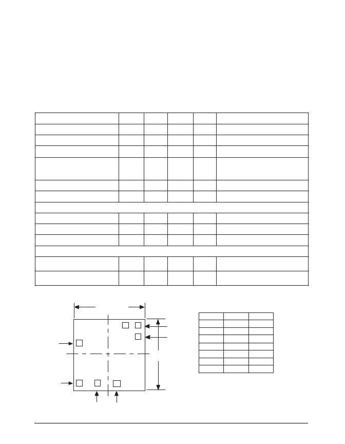
1. Dimensions are in microns unless otherwise noted (mils)
2. Bonding pads are 125 x 125 microns typical
3. Outside dimensions are maximum including scribe area
4. Die thickness is 15 mils +/- 1
5. Pad center coordinates are relative to the die center.
Measured from center of Pads.
PIN
CLK
218.5
HON
418.5
V
418.5
EL2
-178.0
EL1
95.5
COIL
-416.0
V
SS
1397
(55)
Coil
Lamp 2
Lamp 1
Clk.
V
DD
V
SS
Y
X
(0,0)
1143
(45)
HON
SPECIFICATIONS
T= 25
°
C; V
DD
= 3.0V; Lamp Capacitance = 2000pF; Coil = 30 mH at 125 Ohms; External Oscillator = 32768Hz (unless otherwise noted).
ABSOLUTE MAXIMUM RATINGS
These are stress ratings only and functional operation of the device at
these ratings or any other above those indicated in the operation sections
of the specifications below is not implied. Exposure to absolute maximum
rating conditions for extended periods of time may affect reliability.
V
..................................................................................................5.0 V
Input Voltages/Currents
HON (pin 1).........................................-0.5V to (V
+0.5V)
COIL (pin 3)..............................................................60mA
Lamp Outputs...............................................................................250V
PP
Storage Temperature.....................................................-65C to +150C
Power Dissipation Per Package
8-pin NSOIC (derate 6.14mW
o
C above +70
o
C)...................................500mW
8-pin
μ
SOIC (derate 4.85mW
o
C above +70
o
C)....................................390mW
The information furnished herein by Sipex has been carefully reviewed
for accuracy and reliability. Its application or use, however, is solely the
responsibility of the user. No responsibility for the use of this
information is assumed by Sipex, and this information shall not explicitly
or implicitly become part of the terms and conditions of any subsequent
sales agreement with Sipex. Specifications are subject to change
without prior notice. By the sale or transfer of this information, Sipex
assumes no responsibility for any infringement of patents or other rights
of third parties which may result from its use. No license or other
proprietary rights are granted by implication or otherwise under any
patent or patent rights of Sipex Corporation.
BONDING DIAGRAM
X
Y
555.5
555.5
339.5
-555.5
-555.5
-555.5
-416.0
219.0
R
E
T
E
M
A
R
A
P
.
N
I
M
.
P
Y
T
.
X
A
M
S
T
N
U
S
N
O
I
D
N
O
C
V
,
g
a
V
y
p
u
S
D
D
2
0
6
V
,
e
C
y
p
u
S
I
L
O
C
I
D
D
5
0
A
m
V
N
O
H
V
=
D
D
V
3
=
V
,
g
a
V
l
C
L
O
C
V
D
D
6
V
V
L
L
E
,
g
:
W
H
G
a
V
O
L
I
H
t
p
n
N
O
H
N
O
H
f
o
E
n
:
5
2
V
D
D
5
2
0
V
D
D
V
5
2
+
2
V
D
D
5
V
n
o
L
E
,
e
C
N
O
H
1
0
1
0
0
1
μ
A
I
e
C
n
w
o
d
h
S
D
S
I
L
O
C
I
D
D
0
1
0
5
A
n
V
N
O
H
V
0
=
E
V
I
R
D
R
O
T
C
U
D
N
I
f
c
n
e
u
q
e
F
l
C
L
O
C
f
P
M
A
L
2
3
x
2
9
1
8
z
H
z
H
8
6
7
2
3
=
r
s
O
t
p
n
e
y
C
y
D
l
C
5
7
%
I
e
C
l
C
k
a
e
P
L
O
C
-
K
P
0
6
A
m
.
g
e
d
y
b
d
e
e
a
u
G
T
U
P
T
U
O
P
M
A
L
L
E
f
c
n
e
u
q
e
F
p
m
a
L
L
E
P
M
A
L
6
5
2
z
H
z
H
8
6
7
2
3
=
r
s
O
t
p
n
e
g
a
V
t
p
O
k
a
e
P
o
k
a
e
P
0
2
1
0
6
1
V
P
P
相關(guān)PDF資料 |
PDF描述 |
|---|---|
| SP4414 | Low Cost Electroluminescent Lamp Driver |
| SP4414EN | Low Cost Electroluminescent Lamp Driver |
| SP4414EU | Low Cost Electroluminescent Lamp Driver |
| SP4414NEB | Low Cost Electroluminescent Lamp Driver |
| SP4414UEB | Low Cost Electroluminescent Lamp Driver |
相關(guān)代理商/技術(shù)參數(shù) |
參數(shù)描述 |
|---|---|
| SP4412CN | 制造商:Exar Corporation 功能描述:4412CN |
| SP4414 | 制造商:SIPEX 制造商全稱:Sipex Corporation 功能描述:Low Cost Electroluminescent Lamp Driver |
| SP4414EN | 制造商:SIPEX 制造商全稱:Sipex Corporation 功能描述:Low Cost Electroluminescent Lamp Driver |
| SP4414EU | 制造商:SIPEX 制造商全稱:Sipex Corporation 功能描述:Low Cost Electroluminescent Lamp Driver |
| SP4414NEB | 制造商:SIPEX 制造商全稱:Sipex Corporation 功能描述:Low Cost Electroluminescent Lamp Driver |
發(fā)布緊急采購(gòu),3分鐘左右您將得到回復(fù)。