- 您現(xiàn)在的位置:買賣IC網(wǎng) > PDF目錄372193 > SP574BS 12-Bit Sampling A/D Converters PDF資料下載
參數(shù)資料
| 型號: | SP574BS |
| 元件分類: | 串行ADC |
| 英文描述: | 12-Bit Sampling A/D Converters |
| 中文描述: | 12位采樣的A / D轉(zhuǎn)換器 |
| 文件頁數(shù): | 9/15頁 |
| 文件大?。?/td> | 172K |
| 代理商: | SP574BS |

SP574B/674B/1674B/774B
12–Bit Sampling A/D Converters
9
Copyright 2000 Sipex Corporation
Conversion Length
A conversion start transition latches the state of A
0
as shown in
Figure 4
and
Table 1
. The latched state
determines if the conversion stops with 8–bits (A
0
high) or continues for 12–bits (A
low). If all 12–
bits are read following an 8–bit conversion, the
three LSB’s will be a logic “0” and DB
will be a
logic “1”. A
is latched because it is also involved
in enabling the output buffers as explained else-
where. No other control inputs are latched.
Stand–Alone Operation
The simplest interface is a control line connected
to R/C. The other controls must be tied to known
states as follows: CE and 12/8 are wired high, A
0
and CS are wired low. The output data arrives in
words of 12–bits each. The limits on R/C duty
cycle are shown in
Figures 8
and
9
. The duty cycle
may be within and including the extremes shown
in the specifications. In general, data may be read
when R/C is high unless STS is also high, indicat-
ing a conversion is in progress.
Reading Output Data
The output data buffers remain in a high imped-
ance state until the following four conditions are
met: R/C is high, STS is low, CE is high and CS is
low. The data lines become active in response to
these four conditions, and output data according to
the conditions of the control lines 12/8 and A
. The
timing diagram for this process is shown in
Figure
7
. When 12/8 is high, all 12 data outputs become
active simultaneously and the A
input is ignored.
The 12/8 input is usually tied high or low; it is TTL/
CMOS compatible. When 12/8 is low, the output
is separated into two 8–bit bytes as shown below:
BYTE 1
xxxx xxxx
BYTE2
xxxx 0000
MSB
LSB
This configuration makes it easy to connect to an
8–bit data bus as shown in
Figure 5
. The A
control
can be connected to the least significant bit of the
address bus in order to store the output data into
two consecutive memory locations. When A
is
pulled low, the 8 MSB’s are enabled only. When
A
is high, the 8 MSB’s are disabled, bits 4 through
7 are forced to a zero and the four LSB’s are
enabled. The two byte format is “l(fā)eft justified data”
as shown above and can be considered to have a
decimal point or binary to the left of byte 1.
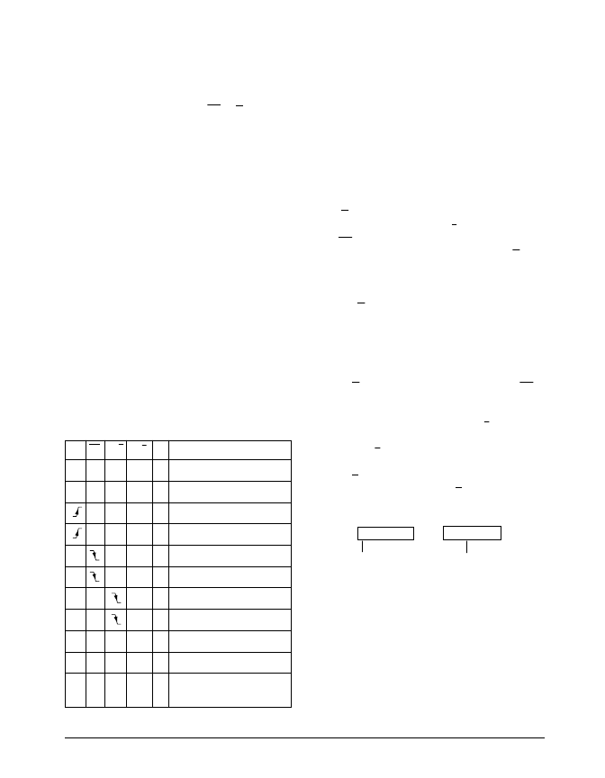
shown in
Table 1
, and the internal control logic is
shown in a simplified schematic in
Figure 4
.
Conversion Start
A conversion may be initiated by a logic transition
on any of the three inputs: CE, CS R/C, as shown
in
Table
1. The last of the three to reach the correct
state starts the conversion, so one, two or all three
may be dynamically controlled. The nominal de-
lay from each is the same and all three may change
state simultaneously. In order to assure that a
particular input controls the start of conversion, the
other two should be setup at least 50ns earlier.
Refer to the convert mode timing specifications.
The Convert Start timing diagram is shown in
Figure 6
.
The output signal STS is the status flag and goes
high only when a conversion is in progress.
While STS is high, the output buffers remain in
a high impedance state so that data can not be
read. Also, when STS is high, an additional Start
Convert will not reset the converter or reinitiate
a conversion. Note, if A
changes state after a
conversion begins, an additional Start Convert
command will latch the new state of A
and
possibly cause a wrong cycle length for that
conversion (8–versus 12–bits).
Table 1. SPx74B Control Input Truth Table
CE CS R/C 12/8 A
0
OPERATION
0
x
x
x
x
None
x
1
x
x
x
None
0
0
x
0
Initiate 12–Bit Conversion
0
0
x
1
Initiate 8–Bit Conversion
1
0
x
0
Initiate 12–Bit Conversion
1
0
x
1
Initiate 8–Bit Conversion
1
0
x
0
Initiate 12–Bit Conversion
1
0
x
1
Initiate 8–Bit Conversion
1
0
1
1
x
Enable 12–Bit Output
1
0
1
0
0
Enable 8 MSB's Only
1
0
1
0
1
Enable 4 LSB's plus 4
Trailing Zeroes
相關(guān)PDF資料 |
PDF描述 |
|---|---|
| SP574BT | 12-Bit Sampling A/D Converters |
| SP1674BA | 12-Bit Sampling A/D Converters |
| SP1674BB | 12-Bit Sampling A/D Converters |
| SP1674BJ | 12-Bit Sampling A/D Converters |
| SP1674BK | 12-Bit Sampling A/D Converters |
相關(guān)代理商/技術(shù)參數(shù) |
參數(shù)描述 |
|---|---|
| SP574BT | 制造商:SIPEX 制造商全稱:Sipex Corporation 功能描述:12-Bit Sampling A/D Converters |
| SP575 | 制造商:未知廠家 制造商全稱:未知廠家 功能描述:低壓壓擴電路 |
| SP5768 | 制造商:ZARLINK 制造商全稱:Zarlink Semiconductor Inc 功能描述:3.0 GHz Low Phase Noise Frequency Synthesiser |
| SP5768KG | 制造商:ZARLINK 制造商全稱:Zarlink Semiconductor Inc 功能描述:3.0 GHz Low Phase Noise Frequency Synthesiser |
| SP5768MP1S | 制造商:ZARLINK 制造商全稱:Zarlink Semiconductor Inc 功能描述:3.0 GHz Low Phase Noise Frequency Synthesiser |
發(fā)布緊急采購,3分鐘左右您將得到回復。