- 您現(xiàn)在的位置:買賣IC網 > PDF目錄372187 > SP6137LEDEB Evaluation Board Manual PDF資料下載
參數(shù)資料
| 型號: | SP6137LEDEB |
| 英文描述: | Evaluation Board Manual |
| 中文描述: | 評估板手冊 |
| 文件頁數(shù): | 10/13頁 |
| 文件大?。?/td> | 142K |
| 代理商: | SP6137LEDEB |

10
Date: 7/28/04 SP6137 Wide Input, 900KHz Synchronous PWM Controll Copyright 2004 Sipex Corporation
thermal improvement can be achieved in the maxi-
mum power dissipation through the proper design
of copper mounting pads on the circuit board. For
example, in a SO-8 package, placing two 0.04
square inches copper pad directly under the pack-
age, without occupying additional board space,
can increase the maximum power from approxi-
mately 1 to 1.2W. For DPAK package, enlarging
the tap mounting pad to 1 square inches reduces the
R
Θ
JA from 96
°
C/W to 40
°
C/W.
APPLICATIONS INFORMATION: Continued
Schottky Diode Selection
When paralleled with the bottom MOSFET, an
optional Schottky diode can improve efficiency
and reduce noises. Without this Schottky diode,
the body diode of the bottom MOSFET con-
ducts the current during the non-overlap time
when both MOSFETs are turned off. Unfortu-
nately, the body diode has high forward voltage
and reverse recovery problem. The reverse re-
covery of the body diode causes additional
switching noises when the diode turns off. The
Schottky diode alleviates these noises and addi-
tionally improves efficiency thanks to its low
forward voltage. The reverse voltage across the
diode is equal to input voltage, and the diode
must be able to handle the peak current equal to
the maximum load current.
The power dissipation of the Schottky diode is
determined by
P
DIODE
= 2V
F
I
OUT
T
NOL
F
S
where
T
NOL
= non-overlap time between GH and GL.
V
F
= forward voltage of the Schottky diode.
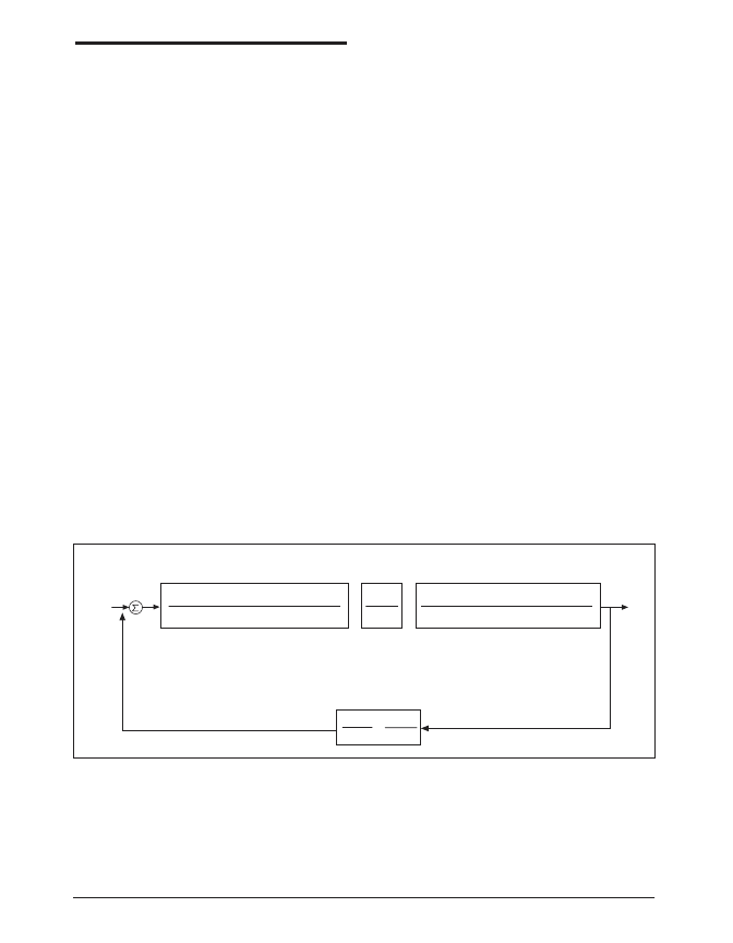
Loop Compensation Design
The open loop gain of the whole system can be
divided into the gain of the error amplifier,
PWM modulator, buck converter output stage,
and feedback resistor divider. In order to cross-
over at the selected frequency FCO, the gain of
the error amplifier has to compensate for the
attenuation caused by the rest of the loop at this
frequency.
(SRz2Cz2+1)(SR1Cz3+1)
(SR
ESR
C
OUT
+ 1)
[S^2LC
OUT
+S(R
ESR
+R
DC
) C
OUT
+1]
V
IN
SR1Cz2(SRz3Cz3+1)(SRz2Cp1+1)
V
RAMP_PP
V
OUT
(Volts)
+
_
V
(Volts)
Notes: R
ESR
= Output Capacitor Equivalent Series Resistance.
R
DC
= Output Inductor DC Resistance.
V
RAMP_PP
= SP6132 Internal RAMP Amplitude Peak to Peak Voltage.
Condition: Cz2 >> Cp1 & R1 >> Rz3
ESR
& R
DC
R
2
V
REF
V
OUT
(R
1
+ R
2
)
or
V
(Volts)
Type III Voltage Loop
Compensation
G
AMP
(s) Gain Block
PWM Stage
G
PWM
Gain
Block
Output Stage
G
OUT
(s) Gain
Block
Voltage Feedback
G
FBK
Gain Block
SP6134 Voltage Mode Control Loop with Loop Dynamic
相關PDF資料 |
PDF描述 |
|---|---|
| SP6138 | Evaluation Board Manual |
| SP6138_06 | Evaluation Board Manual |
| SP6138EB | Evaluation Board Manual |
| SP6138ER1 | Evaluation Board Manual |
| SP6139 | Busway FS Plug-In 600A |
相關代理商/技術參數(shù) |
參數(shù)描述 |
|---|---|
| SP6138 | 制造商:SIPEX 制造商全稱:Sipex Corporation 功能描述:Evaluation Board Manual |
| SP6138_06 | 制造商:SIPEX 制造商全稱:Sipex Corporation 功能描述:Evaluation Board Manual |
| SP6138EB | 功能描述:DC/DC 開關控制器 Synchronous Buck Controller RoHS:否 制造商:Texas Instruments 輸入電壓:6 V to 100 V 開關頻率: 輸出電壓:1.215 V to 80 V 輸出電流:3.5 A 輸出端數(shù)量:1 最大工作溫度:+ 125 C 安裝風格: 封裝 / 箱體:CPAK |
| SP6138ER1 | 制造商:Exar Corporation 功能描述: |
| SP6138ER1/TR | 制造商:SIPEX 制造商全稱:Sipex Corporation 功能描述:Synchronous Buck Controller |
發(fā)布緊急采購,3分鐘左右您將得到回復。