- 您現(xiàn)在的位置:買賣IC網(wǎng) > PDF目錄372187 > SP619EK-L High Current Power Switch PDF資料下載
參數(shù)資料
| 型號: | SP619EK-L |
| 英文描述: | High Current Power Switch |
| 中文描述: | 高電流電源開關(guān) |
| 文件頁數(shù): | 4/7頁 |
| 文件大小: | 427K |
| 代理商: | SP619EK-L |

Jul23-07 Rev K
SP69 High Current Power Switch 2007 Sipex Corporation
4
THEORy OF OPERATION
The SP69 is a switch capable of handling
up to 800mA of current. 7V capability al-
lows the user to have a wide input voltage
range that covers the typical Lithium bat-
tery range as well as higher 5V input volt-
age rails commonly found in USB power.
The SP69 also can be used as a 3V or 5V
power distribution switch. It is intended for
power distribution applications where short
circuits are likely to be encountered.
Short circuit operation
When the SP69 enters a short circuit con-
dition, the switch is disabled. The output
of the SP69 will not restart until the out-
put impedance is greater than 15K. The
enable pin can be used to re-enable the
SP69 into any load condition that is not
a fault condition. Refer to the truth table on
page 4 for more information on the differ-
ent SP69 switch states. The typical deac-
tivation time is about 2ms.
Enable
The enable pin allows easy control of the
SP69. The enable pin should not be en-
abled high prior to a voltage being pres-
ent on the input of the device. The enable
pin should not exceed the input voltage by
more than 0.1V due to an internal ESD di
-
ode. Doing so will affect the operation of
the SP69 and could damage the device.
In a typical application an 80K resistor to
GND should be used on the enable pin.
This resistor will pull the enable low when
an enable signal is not present. This pre-
vents the SP69 from falsely turning on.
The enable pin can also be used to restart
the part into a load condition that is high in
current. Please refer to the truth table on
page 4 for more details.
Inrush Current
The SP69 is a simple resistive switch.
When the switch is turned on into a highly
capacitive load there could be a significant
inrush current that can be encountered.
At 6 volts in, the inrush current was about
250mA into a 00μF capacitor.
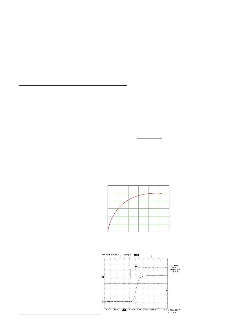
Output Voltage Rise Time
The output voltage of the SP69 has an
output capacitance dependency on the
slope of V
out
. A simple RC circuit is cre-
ated when the switch is turned on.
Equation 1
V(t)=V
o
+V
in
(
-e
(
R
ds
(
on
)
C
out
-t
Where V
o
is initial Voltage condition typi-
cally 0V
V
in
is the input voltage
R
ds
(
on
)
is the switch resistance
C
out
is the output capacitance
For 4.2V V
in
and 00μF output capacitance
we get about 150ns delay in figure 2.
4.17
3.33
2.5
1.67
0.83
00
0.33
0.67
1
1.33
1.67
2
time in uS
V
OUT
This is comparable to actual measured
value in figure 3.
相關(guān)PDF資料 |
PDF描述 |
|---|---|
| SP6200EM5-1.5 | Micropower, 100mA and 200mA CMOS LDO Regulators |
| SP6200EM5-1.8 | Micropower, 100mA and 200mA CMOS LDO Regulators |
| SP6200EM5-2.5 | Micropower, 100mA and 200mA CMOS LDO Regulators |
| SP6200EM5-2.7 | Micropower, 100mA and 200mA CMOS LDO Regulators |
| SP6200EM5-2.85 | Micropower, 100mA and 200mA CMOS LDO Regulators |
相關(guān)代理商/技術(shù)參數(shù) |
參數(shù)描述 |
|---|---|
| SP619EK-L/TR | 功能描述:電源開關(guān) IC - 配電 800mA Current Limit Switch RoHS:否 制造商:Exar 輸出端數(shù)量:1 開啟電阻(最大值):85 mOhms 開啟時間(最大值):400 us 關(guān)閉時間(最大值):20 us 工作電源電壓:3.2 V to 6.5 V 電源電流(最大值): 最大工作溫度:+ 85 C 安裝風(fēng)格:SMD/SMT 封裝 / 箱體:SOT-23-5 |
| SP6200 | 制造商:SIPEX 制造商全稱:Sipex Corporation 功能描述:Micropower, 100mA and 200mA CMOS LDO Regulators |
| SP6200EM5-1.5 | 制造商:SIPEX 制造商全稱:Sipex Corporation 功能描述:Micropower, 100mA and 200mA CMOS LDO Regulators |
| SP6200EM5-1.5/TR | 制造商:SIPEX 制造商全稱:Sipex Corporation 功能描述:Micropower, 100mA and 200mA CMOS LDO Regulators |
| SP6200EM5-1.8 | 制造商:SIPEX 制造商全稱:Sipex Corporation 功能描述:Micropower, 100mA and 200mA CMOS LDO Regulators |
發(fā)布緊急采購,3分鐘左右您將得到回復(fù)。