- 您現(xiàn)在的位置:買賣IC網(wǎng) > PDF目錄372190 > SP6656 High Efficiency 400mA Synchronous Buck Regulator with Bit Programmable Output PDF資料下載
參數(shù)資料
| 型號: | SP6656 |
| 英文描述: | High Efficiency 400mA Synchronous Buck Regulator with Bit Programmable Output |
| 中文描述: | 高效率400mA同步降壓穩(wěn)壓器的可編程輸出位 |
| 文件頁數(shù): | 8/17頁 |
| 文件大小: | 185K |
| 代理商: | SP6656 |

8
Date: 7/9/04
SP6656 High Efficiency 400mA Synchronous Buck Regulator with Bit Programmable Output Copyright 2004 Sipex Corporation
THEORY OF OPERATION
The SP6656 is a high efficiency synchronous
buck regulator with an input voltage range of
+2.7V to +5.5Vand an output that is adjustable
between +1.0V and V
IN
. The SP6656 features a
unique on-time control loop that runs in discon-
tinuous conduction mode (DCM) or continuous
conduction mode (CCM) using synchronous
rectification. Other features include over-tem-
perature shutdown, over-current protection, an
external feedback pin, digitally controlled en-
able and output voltage selection.
The SP6656 operates with a light load quiescent
current of 20
μ
A using a 0.3
PMOS main
switch and a 0.3
NMOS synchronous switch.
It operates with excellent efficiency across the
entire load range, making it an ideal solution for
battery powered applications and low current
step-down conversions. The part smoothly tran-
sitions into a 100% duty cycle under heavy load/
low input voltage conditions.
On-Time Control - Charge Phase
The SP6656 uses a precision comparator and a
minimum on-time to regulate the output voltage
and control the inductor current under normal
load conditions. As the feedback pin drops be-
low the regulation point, the loop comparator
output goes high and closes the main switch.
The minimum on-timer is triggered, setting a
logic high for the duration defined by:
T
ON
= K
ON
V
IN
- V
OUT
where:
K
ON
= 2.25V*
μ
sec constant
V
IN
= V
IN
pin voltage
V
OUT
= V
OUT
pin voltage
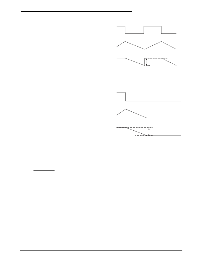
To accommodate the use of ceramic and other
low ESR capacitors, an open loop ramp is added
to the feedback signal to mimic the inductor
current ripple. The following waveforms de-
scribe the ideal ramp operation in both CCM and
DCM operation.
In either CCM or DCM, the negative going
ramp voltage (V
RAMP
in the functional diagram)
is added to FB and this creates the FB's signal.
This FB signal is applied to the negative termi-
nal of the loop comparator. To the positive
terminal of the loop comparator is applied the
REF voltage of 0.8V plus an offset voltage Vos
to compensate for the DC level of V
RAMP
ap-
plied to the negative terminal. The result is an
internal ramp with enough negative going offset
(approximately 50mV) to trip the loop com-
parator whenever FB falls below regulation.
The output of the loop comparator, a rising
VOLOW, causes a SET if BLANK = 0 and
OVR_I = 0. This starts inductor charging
(DRVON = 1) and starts the minimum on-timer.
The minimum on-timer times out and indicates
DRVON can be reset if the voltage loop is
satisfied. If V
OUT
is still below the regulation
point RESET is held low until V
OUT
is above
DRVON
REF, FB
V
OS
REF’
FB’
I(L1)
RAMP: DCM OPERATION
DRVON
REF, FB
V
OS
REF’
FB’
I(L1)
RAMP: CCM OPERATION
相關(guān)PDF資料 |
PDF描述 |
|---|---|
| SP6660CN | 200mA Charge Pump Inverter or Doubler |
| SP6660EB | 200mA Charge Pump Inverter or Doubler |
| SP6660EN | 200mA Charge Pump Inverter or Doubler |
| SP6660EP | 200mA Charge Pump Inverter or Doubler |
| SP6660EU | 200mA Charge Pump Inverter or Doubler |
相關(guān)代理商/技術(shù)參數(shù) |
參數(shù)描述 |
|---|---|
| SP6656_06 | 制造商:SIPEX 制造商全稱:Sipex Corporation 功能描述:High Efficiency 400mA Synchronous Buck Regulator with Dynamically Adjustable Voltage Output |
| SP6656EB | 功能描述:電源管理IC開發(fā)工具 Hi-Efficiency 400mA Sync Buck Regulator RoHS:否 制造商:Maxim Integrated 產(chǎn)品:Evaluation Kits 類型:Battery Management 工具用于評估:MAX17710GB 輸入電壓: 輸出電壓:1.8 V |
| SP6656ER | 制造商:SIPEX 制造商全稱:Sipex Corporation 功能描述:High Efficiency 400mA Synchronous Buck Regulator with Bit Programmable Output |
| SP6656ER/TR | 制造商:SIPEX 制造商全稱:Sipex Corporation 功能描述:High Efficiency 400mA Synchronous Buck Regulator with Bit Programmable Output |
| SP6656ER3 | 制造商:SIPEX 制造商全稱:Sipex Corporation 功能描述:High Efficiency 400mA Synchronous Buck Regulator with Dynamically Adjustable Voltage Output |
發(fā)布緊急采購,3分鐘左右您將得到回復(fù)。