- 您現(xiàn)在的位置:買賣IC網 > PDF目錄372190 > SP6681 High Efficiency Boost Charge Pump Regulator PDF資料下載
參數(shù)資料
| 型號: | SP6681 |
| 英文描述: | High Efficiency Boost Charge Pump Regulator |
| 中文描述: | 高效率升壓充電泵穩(wěn)壓器 |
| 文件頁數(shù): | 7/10頁 |
| 文件大小: | 125K |
| 代理商: | SP6681 |

7
Rev:A Date: 11/20/03
SP6681 High Efficiency Boost Charge Pump Regulator Copyright 2002 Sipex Corporation
P
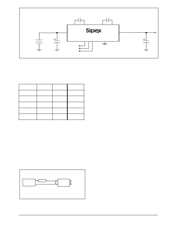
Figure 3. Typical SIM Card Application Circuit for the SP6681
Any standard CMOS logic output is suitable for
driving the C/4 or Cx8 control lines as long as
logic low is less than 0.4V and logic high is
greater than 1.3V.
Efficiency
Power efficiency with the SP6681 charge pump
regulator is improved over standard charge pumps
doubler circuits by the inclusion of an 1.5X
output mode, as described in the Theory of
Operation section. The net result is an increase
in efficiency at battery inputs greater than 3.7 to
3.8V where the SP6681 switches to the 1.5X
mode.
Figure 4. Capacitor Selection Test Circuit
n
K
L
C
n
4
C
n
8
x
C
f
P
M
U
P
t
e
s
e
t
n
X
X
0
z
H
k
8
6
7
3
w
o
w
o
z
H
k
8
6
7
3
z
H
k
8
6
7
3
w
o
h
g
z
H
k
4
1
6
2
z
H
k
8
6
7
3
h
g
w
o
z
H
k
2
9
1
z
H
k
8
6
7
3
h
g
h
g
z
H
k
4
1
6
2
Table 1. Control Line Logic for the Internal Charge
Pump Oscillator
V
OUT
C/4
Cx8
CLK
GND
SP6681
8
CF1P
CF1N
9
CF2P
CF2N
4.7
μ
F
2.2
μ
F
2
10
7
1
6
4
5
3
LithiBattery
V
IN
2.2
μ
F
2.2
μ
F
5.0V output
PHP3631A
1000
μ
F
0.25ohm
0.75” Leads
+
-
V
IN
(p-p)
2.2
μ
F Caps
V
OUT
(p-p)
Capacitor Selection
In order to maintain the lowest output resistance,
input ripple voltage and output ripple voltage,
multi-layer ceramic capacitors with inherently
low ESR are recommended. Refer to Table 2 for
some suggested low ESR capacitors. Tables of
output resistance and ripple voltages for a vari-
ety of input, output and pump capacitors are
included here to use as a guide in capacitor
selection. Measured conditions are with CLK =
32kHz, 5mA output load and all capacitors are
2.2uF except when stated otherwise. A DC
power supply with added 0.25ohm output ESR
was used to simulate a Lithium Ion Battery as
shown in figure 4.
Board Layout
PC board layout is an important design consider-
ation to mitigate switching current effects. High
frequency operation makes PC layout important
for minimizing ground bounc and noise. Com-
ponents should be place as close to the IC as
possible with connections made through short,
low impedance traces. To maximize output
ripple voltage, use a ground plane and solder the
IC's GND pin directly to the ground plane.
相關PDF資料 |
PDF描述 |
|---|---|
| SP6681EU | High Efficiency Boost Charge Pump Regulator |
| SP6682 | High Efficiency Charge Pump Regulator for White LEDs |
| SP6682ER | High Efficiency Charge Pump Regulator for White LEDs |
| SP6682EU | High Efficiency Charge Pump Regulator for White LEDs |
| SP6682UEB | Evaluation Board Manual |
相關代理商/技術參數(shù) |
參數(shù)描述 |
|---|---|
| SP6681EU | 制造商:SIPEX 制造商全稱:Sipex Corporation 功能描述:High Efficiency Boost Charge Pump Regulator |
| SP6681EU/TR | 制造商:SIPEX 制造商全稱:Sipex Corporation 功能描述:High Efficiency Boost Charge Pump Regulator |
| SP6682 | 制造商:SIPEX 制造商全稱:Sipex Corporation 功能描述:High Efficiency Charge Pump Regulator for White LEDs |
| SP6682_06 | 制造商:SIPEX 制造商全稱:Sipex Corporation 功能描述:High Efficiency Charge Pump Regulator for White LEDs |
| SP6682EB | 功能描述:電源管理IC開發(fā)工具 Eval Board for SP6682 Series RoHS:否 制造商:Maxim Integrated 產品:Evaluation Kits 類型:Battery Management 工具用于評估:MAX17710GB 輸入電壓: 輸出電壓:1.8 V |
發(fā)布緊急采購,3分鐘左右您將得到回復。