- 您現(xiàn)在的位置:買賣IC網(wǎng) > PDF目錄372191 > SP674AU 12-Bit Sampling A/D Converters PDF資料下載
參數(shù)資料
| 型號: | SP674AU |
| 元件分類: | 串行ADC |
| 英文描述: | 12-Bit Sampling A/D Converters |
| 中文描述: | 12位采樣的A / D轉(zhuǎn)換器 |
| 文件頁數(shù): | 10/14頁 |
| 文件大小: | 204K |
| 代理商: | SP674AU |

12
Conversion Length
A conversion start transition latches the state of
A
as shown in
Figure 8
and
Table 1
. The latched
state determines if the conversion stops with 8–
bits (A
high) or continues for 12–bits (A
low).
If all 12–bits are read following an 8–bit conver-
sion, the three LSB’s will be a logic “0” and DB
3
will be a logic “1”. A
is latched because it is also
involved in enabling the output buffers as ex-
plained elsewhere. No other control inputs are
latched.
Stand–Alone Operation
The simplest interface is a control line connected
to R/C. The other controls must be tied to known
states as follows: CE and 12/8 are wired high, A
0
and CS are wired low. The output data arrives in
words of 12–bits each. The limits on R/C duty
cycle are shown in
Figures 9
and
10
. The duty
cycle may be within and including the extremes
shown in the specifications. In general, data may
be read when R/C is high unless STS is also high,
indicating a conversion is in progress.
Reading Output Data
The output data buffers remain in a high imped-
ance state until the following four conditions are
met: R/C is high, STS is low, CE is high and CS
is low. The data lines become active in response
to these four conditions, and output data accord-
ing to the conditions of the control lines 12/8 and
A
0
. The timing diagram for this process is shown
in
Figure 11
. When 12/8 is high, all 12 data
outputs become active simultaneously and the
A
input is ignored. The 12/8 input is usually tied
high or low; it is TTL/CMOS compatible. When
12/8 is low, the output is separated into two 8–bit
bytes as shown below:
BYTE 1
xxxx xxxx
BYTE2
xxxx 0000
MSB
LSB
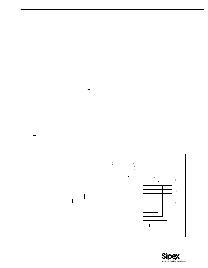
This configuration makes it easy to connect to an
8–bit address bus as shown in
Figure 7
. The A
0
control can be connected to the least significant
bit of the data bus in order to store the output data
into two consecutive memory locations. When
A
is pulled low, the 8 MSB’s are enabled only.
When A
0
is high, the 8 MSB’s are disabled, bits
4 through 7 are forced to a zero and the four
LSB’s are enabled. The two byte format is “l(fā)eft
justified data” as shown above and can be con-
sidered to have a decimal point or binary to the
left of byte 1.
A
may be toggled without damage to the con-
verter at any time. Break–before–make action is
guaranteed between the two data bytes. This
assures that the outputs which are strapped to-
gether in
Figure 11
will never be enabled at the
same time.
In
Figure 11
, it can be seen that a read operation
usually begins after the conversion is complete
and STS is low. If earlier access is needed, the
read can begin no later than the addition of times
t
DD
and t
HS
before STS goes low.
Figure 7. Interfacing SPx74A to 8–Bit Interface Bus
28
27
26
25
24
23
22
21
20
19
18
17
16
15
STS
DB11 (MSB)
DB0 (LSB)
DIG
COM
SPx74A
2
4
A0
ADDRESS BUS
A0
12/8
BUS
相關(guān)PDF資料 |
PDF描述 |
|---|---|
| SP674BA | 12-Bit Sampling A/D Converters |
| SP674BB | 12-Bit Sampling A/D Converters |
| SP674BJ | 12-Bit Sampling A/D Converters |
| SP674BK | 12-Bit Sampling A/D Converters |
| SP674BS | 12-Bit Sampling A/D Converters |
相關(guān)代理商/技術(shù)參數(shù) |
參數(shù)描述 |
|---|---|
| SP674AU/B | 制造商: 功能描述:Analog Digital Converter, Single, 12 Bit, 28 Pin, DIP |
| SP674AU883 | 制造商:SIPEX 制造商全稱:Sipex Corporation 功能描述:12-bit Sampling A/D Converters |
| SP674BA | 制造商:SIPEX 制造商全稱:Sipex Corporation 功能描述:12-Bit Sampling A/D Converters |
| SP674BB | 制造商:SIPEX 制造商全稱:Sipex Corporation 功能描述:12-Bit Sampling A/D Converters |
| SP674BBS | 制造商:Exar Corporation 功能描述: |
發(fā)布緊急采購,3分鐘左右您將得到回復(fù)。