- 您現(xiàn)在的位置:買賣IC網(wǎng) > PDF目錄372191 > SP674BJ 12-Bit Sampling A/D Converters PDF資料下載
參數(shù)資料
| 型號(hào): | SP674BJ |
| 元件分類: | 串行ADC |
| 英文描述: | 12-Bit Sampling A/D Converters |
| 中文描述: | 12位采樣的A / D轉(zhuǎn)換器 |
| 文件頁數(shù): | 8/14頁 |
| 文件大小: | 204K |
| 代理商: | SP674BJ |

10
signals between ground traces and cross digital
lines at right angles only.
Grounding Considerations
Any ground path from the analog and digital
ground should be as low resistance as possible to
accommodate the ground currents present with
this device.
The analog ground current is approximately 6mA
DC while the digital ground is 3mA DC. The
analog and digital common pins should be tied
together as close to the package as possible to
guarantee best performance. The code–depen-
dent currents flow through the V
and V
terminals and not through the analog and digital
common pins.
Power Supplies
The supply voltages for the
SPx74A
must be
kept as quiet as possible from noise pickup and
also regulated from transients or drops. Because
the part has 12–bit accuracy, voltage spikes on
the supply lines can cause several LSB devia-
tions on the output. Switching power supply
noise can be a problem. Careful filtering and
shielding should be employed to prevent the
noise from being picked up by the converter.
Capacitor bypass pairs are needed from each
supply pin to its respective ground to filter noise
and counter the problems caused by the varia-
tions in supply current. A 10
μ
F tantalum and a
0.1
μ
F ceramic type in parallel between V
(pin 1) and digital common (pin15), and V
CC
(pin
7) and analog common (pin 9) is sufficient. V
is generated internally so pin 11 may be grounded
or connected to a negative supply if the
SPx74A
is being used to upgrade an already existing
design.
CALIBRATION AND CONNECTION
PROCEDURES
Unipolar
The calibration procedure consists of adjusting
the converter’s most negative output to its ideal
value for offset adjustment, and then adjusting
the most positive output to its ideal value for gain
adjustment.
Starting with offset adjustment and referring to
Figure 4
, the midpoint of the first LSB increment
should be positioned at the origin to get an output
code of all 0s. To do this, an input of +
1
LSB or
+1.22mV for the 10V range and +2.44mV for the
20V range should be applied to the
SPx74A
.
Adjust the offset potentiometer R
for code tran-
sition flickers between 0000 0000 0000 and
0000 0000 0001.
The gain adjustment should be done at positive
full scale. The ideal input corresponding to the
last code change is applied. This is 1
1
LSB
below the nominal full scale which is +9.9963V
for the 10V range and +19.9927V for the 20V
range. Adjust the gain potentiometer R
for flicker
between codes 1111 1111 1110 and 1111 1111
1111. If calibration is not necessary for the
intended application, replace R
with a 50
, 1%
metal film resistor and remove the network ana-
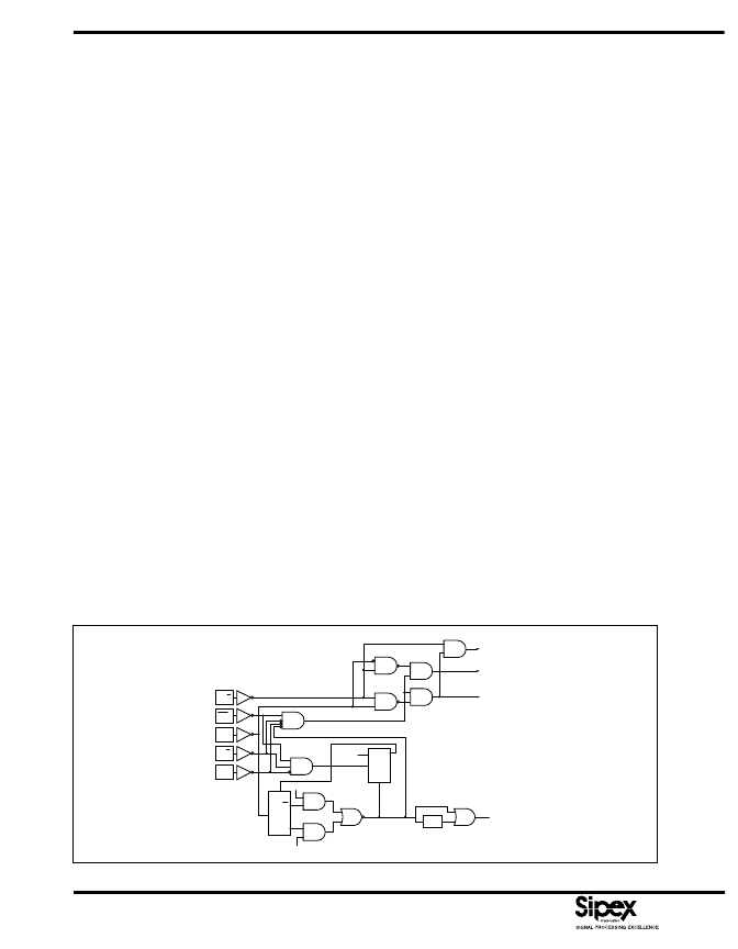
Figure 6. SPx74A Control Logic
STS
DELAY
R
CK
Q
D
H
D
CK
Q
Q
EOC8
EOC12
CE
R/C
A0
CS
12/8
READ CONTROL
A0 LATCH
INPUT BUFFERS
NIBBLE B ZERO
OVERRIDE
NIBBLE A, B
NIBBLE C
相關(guān)PDF資料 |
PDF描述 |
|---|---|
| SP674BK | 12-Bit Sampling A/D Converters |
| SP674BS | 12-Bit Sampling A/D Converters |
| SP674BT | 12-Bit Sampling A/D Converters |
| SP6828-5EK | +3V Low Power Voltage Inverters |
| SP6828EK | +3V Low Power Voltage Inverters |
相關(guān)代理商/技術(shù)參數(shù) |
參數(shù)描述 |
|---|---|
| SP674BK | 制造商:SIPEX 制造商全稱:Sipex Corporation 功能描述:12-Bit Sampling A/D Converters |
| SP674BKP | 制造商:Exar Corporation 功能描述:Analog Digital Converter, Single, 12 Bit, 28 Pin, DIP |
| SP674BS | 制造商:SIPEX 制造商全稱:Sipex Corporation 功能描述:12-Bit Sampling A/D Converters |
| SP674BT | 制造商:SIPEX 制造商全稱:Sipex Corporation 功能描述:12-Bit Sampling A/D Converters |
| SP67596 | 制造商:L COM 功能描述:CA DB50F DB50M CST WIR 2.5F 制造商:L-com Inc 功能描述:CA DB50F DB50M CST WIR 2.5F |
發(fā)布緊急采購,3分鐘左右您將得到回復(fù)。