- 您現在的位置:買賣IC網 > PDF目錄372191 > SP6828-5TR +3V Low Power Voltage Inverters PDF資料下載
參數資料
| 型號: | SP6828-5TR |
| 英文描述: | +3V Low Power Voltage Inverters |
| 中文描述: | 3V的低功率高壓變頻器 |
| 文件頁數: | 10/17頁 |
| 文件大小: | 258K |
| 代理商: | SP6828-5TR |

10
SP6828DS/11 SP6828/6829 +3V Low Power Voltage Inverter Copyright 2000 Sipex Corporation
DESCRIPTION
The
SP6828/6829
devices are CMOS Charge
Pump Voltage Converters that can be used to
invert a +1.15V to +4.2V input voltage. These
devices are ideal for designs involving battery-
powered and/or board level voltage conversion
applications.
The typical operating frequency of the
SP6828
is 12kHz. The typical operating frequency of the
SP6829
is 35kHz. The
SP6828
has a typical
operating current of 20
μ
A and the
SP6829
operates at 40
μ
A. Both devices can output 25mA
with a voltage drop of 500mV. The devices are
ideal for designs using +3.3V or +3.6V lithium
ion batteries such as cell phones, PDAs, medical
instruments, and other portable equipment. The
SP6828/6829
devices combine a high efficiency
with a low quiescent current.
THEORY OF OPERATION
The
SP6828/6829
devices should theoretically
produce an inverted input voltage. In real world
applications, there are small voltage drops at the
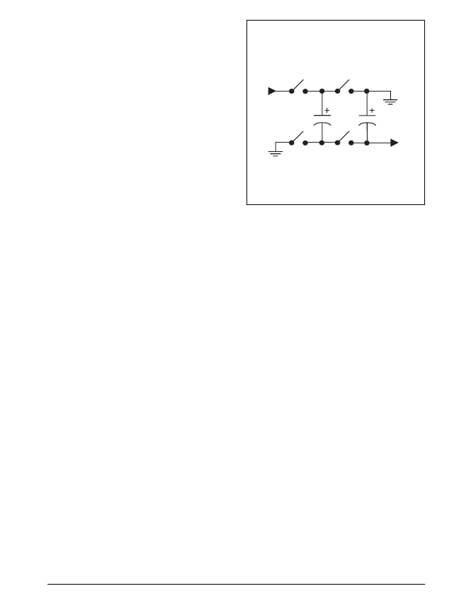
output that reduce efficiency. The circuit of an
ideal voltage inverter can be found in
Figure 21
.
The voltage inverters require two external
capacitors to store the charge. A description of
the two phases follows:
Phase 1
In the first phase of the clock cycle, switches S2
and S4 are opened and S1 and S3 closed. This
connects the flying capacitor, C1, from V
to
ground. C1 charges up to the input voltage applied
at V
IN
.
Phase 2
In the second phase of the clock cycle, switches
S2 and S4 are closed and S1 and S3 are opened.
This connects the flying capacitor, C1, in parallel
with the output capacitor, C2. The charge stored
in C1 is now transferred to C2. Simultaneously,
the negative side of C2 is connected to V
and
the positive side is connected to ground. With
the voltage across C2 smaller than the voltage
across C1, the charge flows from C1 to C2 until
the voltage at the V
OUT
equals -V
IN
.
Charge-Pump Output
The output of the
SP6828/6829
devices is not
regulated and therefore is dependent on the
output resistance and the amount of load current.
As the load current increases, losses may slightly
increase at the output and the voltage may become
slightly more positive. The loss at the negative
output, V
, equals the current draw, I
, from
V
times the negative converter's source
resistance, R
S
:
V
LOSS
= I
OUT
x R
S
.
The actual inverted output voltage at V
OUT
will
equal the inverted voltage difference of V
IN
and
V
LOSS
:
V
OUT
= -(V
IN
- V
LOSS
).
Efficiency
Theoretically, the total power loss of a switched
capacitor voltage converter can be summed up as
follows:
∑
P
LOSS
= P
INT
+ P
CAP
+ P
CONV
,
where P
is the total power loss, P
is the total
internal loss in the IC including any losses in the
MOSFET switches, P
CAP
is the resistive loss of
Figure 21. Circuit for an Ideal Voltage Inverter
C1
C2
S1
S3
S4
S2
V
OUT
V
IN
V
OUT
= -V
IN
相關PDF資料 |
PDF描述 |
|---|---|
| SP6829EK | +3V Low Power Voltage Inverters |
| SP6829TR | +3V Low Power Voltage Inverters |
| SP6830 | Low Power Voltage Inverters With Shutdown |
| SP6831TR | Low Power Voltage Inverters With Shutdown |
| SP6830EK | Low Power Voltage Inverters With Shutdown |
相關代理商/技術參數 |
參數描述 |
|---|---|
| SP6828EK | 制造商:SIPEX 制造商全稱:Sipex Corporation 功能描述:+3V Low Power Voltage Inverters |
| SP6828EK/TR | 制造商:SIPEX 制造商全稱:Sipex Corporation 功能描述:+3V Low Power Voltage Inverters |
| SP6828TR | 制造商:SIPEX 制造商全稱:Sipex Corporation 功能描述:+3V Low Power Voltage Inverters |
| SP6829 | 制造商:SIPEX 制造商全稱:Sipex Corporation 功能描述:+3V Low Power Voltage Inverters |
| SP6829EK | 制造商:SIPEX 制造商全稱:Sipex Corporation 功能描述:+3V Low Power Voltage Inverters |
發(fā)布緊急采購,3分鐘左右您將得到回復。