- 您現(xiàn)在的位置:買賣IC網(wǎng) > PDF目錄372194 > SP782CT Programmable Charge Pump PDF資料下載
參數(shù)資料
| 型號: | SP782CT |
| 英文描述: | Programmable Charge Pump |
| 中文描述: | 可編程電荷泵 |
| 文件頁數(shù): | 9/16頁 |
| 文件大?。?/td> | 224K |
| 代理商: | SP782CT |
9
SP782/SP784 DS/08
SP782/784 Programmable Charge Pump
Copyright 2000 Sipex Corporation
V
receives a continuous charge from either C
1
or C
. With the C1 capacitor charged to 5V, the
cycle begins again.
Phase 3
— V
charge storage — The third phase of the
clock is identical to the first phase — the charge
transferred in C
produces –5V in the negative
terminal of C
, which is applied to the negative
side of capacitor C
. Since C
voltage potential across C
is l0V. For the 5V
output, C
potential on C
2
is only +5V.
+
is at +5V, the
+
is connected to ground so that the
Phase 4
— V
transfer — The fourth phase of the
clock connects the negative terminal of C
to
ground and transfers the generated l0V or the
generated 5V across C
to C
, the V
storage
capacitor. Again, simultaneously with this, the
positive side of capacitor C
is switched to +5V
and the negative side is connected to ground,
and the cycle begins again.
Since both V
DD
and V
are separately gener-
ated from V
in a no–load condition, V
and
V
will be symmetrical. Older charge pump
approaches that generate V
–
from V
+
will show
a decrease in the magnitude of V
–
compared to
V
+
due to the inherent inefficiencies in the
design.
V
CC
= +5V
–5V
–5V
+5V
V
DD
Storage Capacitor
C
1
C
2
C
4
+
+
+
–
–
–
V
SS
Storage Capacitor
C
3
+
–
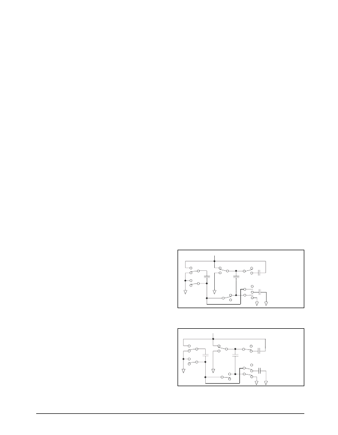
Figure 3. Charge Pump Phase 1 for
±
5V.
V
CC
= +5V
+5V
V
DD
Storage Capacitor
C
1
C
2
C
4
+
+
+
–
–
–
V
SS
Storage Capacitor
C
3
+
–
–5V
Figure 2. Charge Pump Phase 1 for
±
10V.
THEORY OF OPERATION
The
SP782/784's
charge pump design is based
on
Sipex's
original patented charge pump de-
sign (5,306,954) which uses a four–phase volt-
age shifting technique to attain symmetrical
10V power supplies. In addition, the
SP782/
784
charge pump incorporates a "program-
mable" feature that produces an output of
±
10V
or
±
5V for V
and V
by two control pins, D0
and D1. The charge pump requires external
capacitors to store the charge. Figure 1 shows
the waveform found on the positive and nega-
tive side of capcitor C2. There is a free–running
oscillator that controls the four phases of the
voltage shifting. A description of each phase
follows.
Phase 1 (
±
10V)
— V
charge storage — During this phase of
the clock cycle, the positive side of capacitors
C
and C
are initially charged to +5V. C
then switched to ground and the charge on C
is transferred to C
+5V, the voltage potential across capacitor C
2
is now 10V.
+
is
–
–
. Since C
+
is connected to
Phase 1 (
±
5V)
— V
& V
charge storage and transfer —
With the C
1
and C
capacitors initially charged
to +5V, C
charge on C
capacitor. Simultaneously the C
to ground and 5V charge on C
2
to the V
DD
storage capacitor.
+
is then switched to ground and the
–
is transferred to the V
storage
–
is switched
+
is transferred
Phase 2 (
±
10V)
— V
transfer — Phase two of the clock
connects the negative terminal of C
to the V
storage capacitor and the positive terminal of
C
to ground, and transfers the generated –l0V
or the generated –5V to C
. Simultaneously,
the positive side of capacitor C
is switched to
+5V and the negative side is connected to
ground.
Phase 2 (
±
5V)
— V
& V
charge storage — C
reconnected to V
to recharge the C
1
capacitor. C
connected to C
.
The 5V charge from Phase 1 is
now transferred to the V
SS
storage capacitor.
+
is
+
is switched to ground and C
–
is
相關(guān)PDF資料 |
PDF描述 |
|---|---|
| SP784 | Programmable Charge Pump |
| SP784CP | Programmable Charge Pump |
| SP784CT | Programmable Charge Pump |
| SP78L12N1-L | 100mA 3-Terminal Positive Voltage Regulator |
| SP78L12N1-L-TR | 100mA 3-Terminal Positive Voltage Regulator |
相關(guān)代理商/技術(shù)參數(shù) |
參數(shù)描述 |
|---|---|
| SP784 | 制造商:SIPEX 制造商全稱:Sipex Corporation 功能描述:Programmable Charge Pump |
| SP784CP | 制造商:SIPEX 制造商全稱:Sipex Corporation 功能描述:Programmable Charge Pump |
| SP784CT | 制造商:SIPEX 制造商全稱:Sipex Corporation 功能描述:Programmable Charge Pump |
| SP7875 | 制造商:SIPAT 制造商全稱:SIPAT 功能描述:SAW Filter Electrical Characteristic |
| SP78K0 | 制造商:未知廠家 制造商全稱:未知廠家 功能描述:Two Great Forces in the 8-bit Realm Pamphlet | Pamphlet[09/2002] |
發(fā)布緊急采購,3分鐘左右您將得到回復(fù)。