- 您現(xiàn)在的位置:買賣IC網(wǎng) > PDF目錄372198 > SP8121KP Monolithic, 12-Bit Data Acquisition System PDF資料下載
參數(shù)資料
| 型號(hào): | SP8121KP |
| 英文描述: | Monolithic, 12-Bit Data Acquisition System |
| 中文描述: | 單片,12位數(shù)據(jù)采集系統(tǒng) |
| 文件頁數(shù): | 2/13頁 |
| 文件大小: | 168K |
| 代理商: | SP8121KP |

SP8121DS/02
SP8121 Monolithic, 12-Bit Data Acquisition System
2
Copyright 2000 Sipex Corporation
ABSOLUTE MAXIMUM RATINGS
V
CC
to Common Ground .............................................. 0V to +16.5V
V
to Common Ground ............................................... 0V to +7V
Analog Common to Digital Common Ground ...............-0.5V to +1V
Digital Inputs to Common Ground .................... -0.5V to V
LOGIC
+0.5V
Digital Outputs to Common Ground ................. -0.5V to V
+0.5V
Multiplexer Analog Inputs......................................-16.5V to +31.5V
Gain and Offset Adjustment ................................ -0.5V to V
+0.5V
Analog Input Maximum Current ........................................... 100mA
Temperature with Bias Applied ............................. -55
°
C to +125
°
C
Storage Temperature ............................................ -65
°
C to +150
°
C
Lead Temperature, Soldering .................................... 300
°
C, 10sec
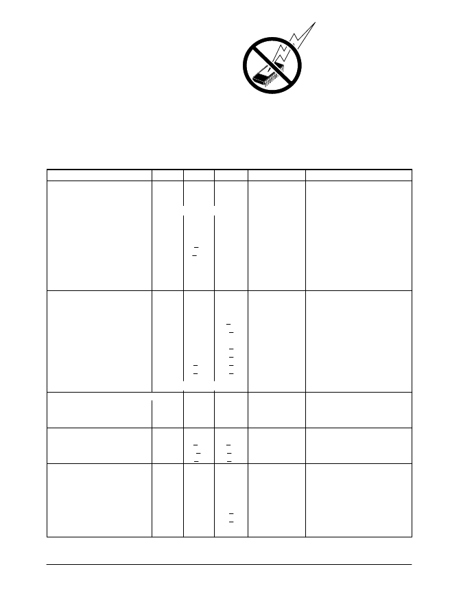
CAUTION:
ESD (ElectroStatic Discharge) sensitive
device. Permanent damage may occur on
unconnected devices subject to high energy
electrostatic fields. Unused devices must be
stored in conductive foam or shunts.
Personnel should be properly grounded prior
to handling this device. The protective foam
should be discharged to the destination
socket before devices are removed.
SPECIFICATIONS
(T
A
= 25
°
C and nominal supply voltages unless otherwise noted)
MIN.
TYP.
MAX.
UNIT
CONDITIONS
ANALOG INPUTS
Input Voltage Range
Multiplexer Inputs
Configuration
Input Impedance
ON Channel
OFF Channel
Input Bias Current/Channel
0 to +5
V
8
Single-ended
10
9
10
10
+10
+250
Parallel with 30pF
Parallel with 5pF
25
°
C
-55
°
C to +125
°
C
nA
nA
Crosstalk
OFF to ON Channel
-90
-80
-70
dB
dB
dB
10kHz, 0V to +5V
Pk-to-pk
50kHz, 0V to +5V
Pk-to-pk
100kHz, 0V to +5V
Pk-to-pk
ACCURACY
Resolution
Linearity Error
–K
–J
Differential Non-Linearity
–K
–J
Offset Error
Gain Error
No Missing Codes
–K
TRANSFER CHARACTERISTICS
Throughput Rate
MUX Settling/Acquisition
A/D Conversion
STABILITY
Linearity
Offset
Gain
DIGITAL INPUTS
Capacitance
Logic Levels
V
IH
V
IL
I
IH
I
IL
12
Bits
+0.5
+1
LSB
LSB
+1
+2
+4
+1
LSB
LSB
LSB
+0.5
+0.3
Adjustable to zero
Adjustable to zero
%FSR
Guaranteed
100
kHz
μ
s
μ
s
1.9
8.1
+0.5
+5
+10
+2.5
+25
+50
ppm/
°
C
ppm/
°
C
ppm/
°
C
5
pF
+2.4
-0.5
+5.5
+0.8
+5
+5
V
V
μ
A
μ
A
相關(guān)PDF資料 |
PDF描述 |
|---|---|
| SP8121KS | CAP ELECT 1UF 50V KK RADIAL |
| SP8121 | Monolithic, 12-Bit Data Acquisition System |
| SP8127NDG | V7 Series Miniature Basic Switch, Single Pole Double Throw Circuitry, 21 A at 277 Vac, Pin Plunger Actuator, 2,21 N [7.9 oz] Maximum Operating Force, Silver Contacts, Quick Connect Termination |
| SP8127N | High Speed Differential APC Amplifier |
| SP813LEP | Low Power Microprocessor Supervisory Circuits |
相關(guān)代理商/技術(shù)參數(shù) |
參數(shù)描述 |
|---|---|
| SP8121KS | 制造商:SIPEX 制造商全稱:Sipex Corporation 功能描述:Monolithic, 12-Bit Data Acquisition System |
| SP8126 | 制造商:SIPEX 制造商全稱:Sipex Corporation 功能描述:High Speed Differential APC Amplifier |
| SP8126B | 制造商:SIPEX 制造商全稱:Sipex Corporation 功能描述:High Speed Differential APC Amplifier |
| SP8126CB-3 | 制造商:SIPEX 制造商全稱:Sipex Corporation 功能描述:High Speed Differential APC Amplifier |
| SP8127 | 制造商:SIPEX 制造商全稱:Sipex Corporation 功能描述:High Speed Differential APC Amplifier |
發(fā)布緊急采購,3分鐘左右您將得到回復(fù)。