- 您現(xiàn)在的位置:買賣IC網(wǎng) > PDF目錄372201 > SP9500KS 12-Bit, Voltage Output D/A Converter PDF資料下載
參數(shù)資料
| 型號: | SP9500KS |
| 英文描述: | 12-Bit, Voltage Output D/A Converter |
| 中文描述: | 12位電壓輸出D / A轉(zhuǎn)換 |
| 文件頁數(shù): | 4/9頁 |
| 文件大?。?/td> | 157K |
| 代理商: | SP9500KS |

SP9500DS/04
SP9500 12-Bit, Voltage Output D/A Converter
4
Copyright 2000 Sipex Corporation
THEORY OF OPERATION
The
SP9500
consists of four main functional
blocks – the input shift register, DAC register,
12-Bit D/A converter and a output buffer
amplifier,
Figure 1
.
The input shift register is used to convert the
serial input data stream to a parallel 12–Bit
digital word. The input data is shifted on posi-
tive clock (SCLK) edges when the Chip Select
(CS) signal is in the “l(fā)ow” state. The MSB is
loaded first and LSB last. No shifting of the
input data occurs when the Chip Select (CS)
signal is in the “high” state.
The DAC register is used to store the digital
word which is sent to the R–2R DAC. Its value
is updated on the positive transition of the Chip
Select (CS) signal.
The 12–Bit D/A converter is an “inverted” R-2R
ladder network. The DAC itself is implemented
with precision thin-film resistors and CMOS
transmission gate switches. The resistor net-
work is laser-trimmed to achieve better than 12–
Bit accuracy. The D/A converter is used to
convert the 12-bit input word to a precision
voltage.
The operational amplifier is a rail-to-rail input,
rail-to-rail output CMOS amplifier. It is capable
of supplying 1mA of load current in the 1.5 to
3.5 output voltage range. The initial offset volt-
age is laser-trimmed to improve accuracy. Set-
tling time is 7.5
μ
s for a full scale output transi-
tion to 0.012% accuracy.
INPUT
OUTPUT
MSB
LSB
1111
1111
1111
V
REF
- 1 LSB
V
REF
- 2 LSB
AGND + 1 LSB
1111
1111
1110
0000
0000
0001
0000
0000
0000
AGND
(V
REF
-AGND)
2
12
1 LSB =
Table 1. Binary Coding
FEATURES...
The
SP9500
is a low power 12–Bit Digital-to-
Analog Converter. The converter features 0.5 to
4.5 volt output swings with a single +5V supply.
The input coding format used is standard binary,
Table 1
.
This Digital-to Analog Converter uses a stan-
dard 3–wire interface compatible with SPI
,
QSPI
and Microwire
. The output settling
time is specified at 7.5
μ
s to full 12-bit accuracy
when driving a 10K
, 10pF load combination.
The
SP9500
Digital-to-Analog Converter is
ideally suited for applications such as ATE,
process controllers, robotics and instrumenta-
tion. The
SP9500
is available in an 8-pin 0.15"
SOIC and 0.3" PDIP packages, specified over
commercial and industrial temperature ranges.
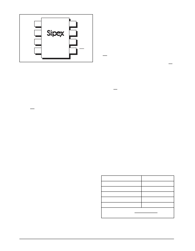
PIN ASSIGNMENTS
Pin 1- V
OUT
- Voltage Output.
Pin 2- V
DD
- +5V Power Supply Input.
Pin 3- SCLK - Serial Clock Input.
Pin 4- D
IN
- Serial Data Input.
Pin 5- CS - Chip Select Input.
Pin 6 - DGND - Digital Ground
Pin 7- AGND - Analog Ground.
Pin 8- V
REF
- Reference Input.
V
OUT
1
2
3
4
8
7
6
5
V
DD
D
IN
V
REF
DGND
CS
AGND
SCLK
SP9500
PINOUT – 8-PIN PLASTIC DIP & SOIC
相關PDF資料 |
PDF描述 |
|---|---|
| SP9502 | Dual, 12-Bit, Voltage Output D/A Converter |
| SP9502JN | Dual, 12-Bit, Voltage Output D/A Converter |
| SP9502JS | Dual, 12-Bit, Voltage Output D/A Converter |
| SP9502KN | Dual, 12-Bit, Voltage Output D/A Converter |
| SP9502KS | Dual, 12-Bit, Voltage Output D/A Converter |
相關代理商/技術參數(shù) |
參數(shù)描述 |
|---|---|
| SP9501 | 制造商:SIPEX 制造商全稱:Sipex Corporation 功能描述:12-Bit, Voltage Output D/A Converter |
| SP9501AN | 制造商:SIPEX 制造商全稱:Sipex Corporation 功能描述:12-Bit, Voltage Output D/A Converter |
| SP9501AS | 制造商:SIPEX 制造商全稱:Sipex Corporation 功能描述:12-Bit, Voltage Output D/A Converter |
| SP9501BN | 制造商:SIPEX 制造商全稱:Sipex Corporation 功能描述:12-Bit, Voltage Output D/A Converter |
| SP9501BS | 制造商:SIPEX 制造商全稱:Sipex Corporation 功能描述:12-Bit, Voltage Output D/A Converter |
發(fā)布緊急采購,3分鐘左右您將得到回復。