- 您現(xiàn)在的位置:買賣IC網(wǎng) > PDF目錄372201 > SP9504KP Quad, 12-Bit, Voltage Output D/A Converter PDF資料下載
參數(shù)資料
| 型號: | SP9504KP |
| 英文描述: | Quad, 12-Bit, Voltage Output D/A Converter |
| 中文描述: | 四,12位電壓輸出D / A轉(zhuǎn)換 |
| 文件頁數(shù): | 5/11頁 |
| 文件大?。?/td> | 184K |
| 代理商: | SP9504KP |

SP9504DS/03
SP9504 Quad, 12-Bit, Voltage Output D/A Converter
5
Copyright 2000 Sipex Corporation
FEATURES
The
SP9504
is a low–power replacement for the
popular SP9345, Quad 12-Bit Digital-to-Analog
Converter. This Quad, Voltage Output, 12-Bit Digi-
tal-to-Analog Converter features
±
4.5V output swings
when using
±
5 volt supplies. The input coding format
used is standard offset binary,
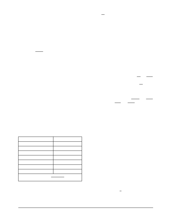
Table 1
.
The converter utilizes double-buffering on each of the
12 parallel digital inputs, for easy microprocessor
interface. Each 12-bit DAC is independently addres-
sable and all DAC
S
may be simultaneously updated
using a single XFER command. The output settling-
time is specified at 4
μ
s to full 12–bit accuracy when
driving a 5Kohm, 50pF load combination. The
SP9504
, Quad 12-Bit Digital-to-Analog Converter is
ideally suited for applications such as ATE, process
controllers, robotics, and instrumentation. The
SP9504
is available in 28–pin plastic DIP or SOIC packages,
specified over the commercial (0
°
C to +70
°
C)
temperature range.
THEORY OF OPERATION
The
SP9504
consists of five main functional blocks
— input data multiplexer, data registers, control logic,
four 12-bit D/A converters, and four bipolar output
voltage amplifiers. The input data multiplexer is
designed to interface to either 12- or 8-bit micropro-
cessor data busses. The input data format
is controlled
by the B1/B2 signal — a logic “1” selects the 12-bit
mode, while a logic “0” selects the 8-bit mode. In the
12-bit mode the data is transferred to the input registers
without changes in its format. In the 8-bit mode, the
four least significant bits (LSBs) are connected to the
four most significant bits (MSBs), allowing an 8-bit
MSB-justified interface. All data inputs are enabled
using the CS signal in both modes. The digital inputs
are designed to be both TTL and 5V CMOS compat-
ible.
In order to reduce the DAC full scale output sensitivity
to the large weighting of the MSB’s found in conven-
tional R-2R resistor ladders, the 3 MSB’s are decoded
into 8 equally weighted levels. This reduces the
contribution of each bit by a factor of 4, thus, reducing
the output sensitivity to mismatches in resistors and
switches by the same amount. Linearity errors and
stability are both improved for the same reasons.
Each D/A converter is separated from the data bus by
two registers, each consisting of level-triggered latches,
Figure 1
. The first register (input register) is 12-bits
wide. The input register is selected by the address
input A
and A
, and is enabled by the CS and WR1
signals. In the 8-bit mode, the enable signal to the 8
MSB’s is disabled by a logic low on B1/B2 to allow
the 4 LSB’s to be updated. The second register (DAC
register), accepts the decoded 3 MSB’s plus the 9
LSB’s. The four DAC registers are updated simulta-
neously for all DAC’s using the XFER and WR2
signals. Using the CLR and WR2 signals or the
power-on-reset, (enabled when the power is switched
on) the DAC registers are set to 1000 0000 0000 and
the DAC outputs will settle to 0V.
Using the control logic inputs, the user has full control
of address decoding, chip enable, data transfer and
clearing of the DAC’s. The control logic inputs are
level triggered, and like the data inputs, are TTL and
CMOS compatible. The truth table (
Table 2
) shows
the appropriate functions associated with the states of
the control logic inputs.
The DACs themselves are implemented with a preci-
sion thin–film resistor network and CMOS transmis-
sion gate switches. Each D/A converter is used to
convert the 12–bit input from its DAC register to a
precision voltage.
The bipolar voltage output of the
SP9504
is created
on-chip from the DAC Voltage Output (V
) by
using an operational amplifier and two feedback
resistors connected as shown in
Figure 2
. This
configuration produces a +4.5V bipolar output range
with standard offset binary coding.
INPUT
OUTPUT
MSB
LSB
1111
1111
1111
VREF - 1 LSB
1111
1111
1110
VREF - 2 LSB
1000
0000
0001
0 + 1 LSB
1000
0000
0000
0
0000
0000
0001
-VREF + 1 LSB
0000
0000
0000
-VREF
2V
REF
2
12
1 LSB =
Table 1. Offset Binary Coding
相關(guān)PDF資料 |
PDF描述 |
|---|---|
| SP9504KS | Quad, 12-Bit, Voltage Output D/A Converter |
| SP9600BN | 12-Bit, Low Power Voltage Output D/A Converter |
| SP9600BS | 12-Bit, Low Power Voltage Output D/A Converter |
| SP9600JN | 12-Bit, Low Power Voltage Output D/A Converter |
| SP9600JS | 12-Bit, Low Power Voltage Output D/A Converter |
相關(guān)代理商/技術(shù)參數(shù) |
參數(shù)描述 |
|---|---|
| SP9504KS | 制造商:SIPEX 制造商全稱:Sipex Corporation 功能描述:Quad, 12-Bit, Voltage Output D/A Converter |
| SP959B | 制造商:SIPAT 制造商全稱:SIPAT 功能描述:DECT RF Filters |
| SP959B01-TD01 | 制造商:未知廠家 制造商全稱:未知廠家 功能描述:China Electronics Technology Group Corporation No.26 Research Institute |
| SP9600 | 制造商:SIPEX 制造商全稱:Sipex Corporation 功能描述:12-Bit, Low Power Voltage Output D/A Converter |
| SP9600AN | 制造商:SIPEX 制造商全稱:Sipex Corporation 功能描述:12-Bit, Low Power Voltage Output D/A Converter |
發(fā)布緊急采購,3分鐘左右您將得到回復(fù)。